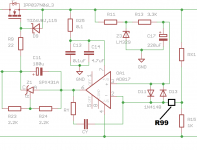
Hidden in plain sight: the attachment to post 86 shows a resistor, which you have omitted in the schematic of post 97.
I've drawn this resistor as "R99" below.
Your frequency compensation scheme connects RY+CY between a low impedance point (the opamp output pin) and a high impedance point (the VIN- pin). Unfortunately when you dial in a different output voltage by changing the ratio RX1-to-R15, you will be changing the impedance at VIN-. Thus when you change the output voltage, you change the frequency compensation of the control system (!). No es bueno.
The simplest fix is to modify both RX1 and R15 when you implement a different output voltage. For each desired output voltage simply choose RX1 and R15 values that (a) give the output you want, and also (b) maintain the impedance at VIN- at one certain specific value. Two requirements, two adjustable parameters (the two resistor values), therefore it is do-able. You can either write and solve the equations using algebra, or just set up a little Excel spreadsheet and dink around with resistor values manually until both requirements are met within an error tolerance you can live with.
But that's not the fix that I implemented in my design. Instead I added a series resistor R99. Now the impedance at VIN- is (R99 + (RX1 // R15)). By making R99 more than 2X larger than (RX1 // R15), the total is relatively insensitive to changes in RX1 and/or R15.
edit- no MMBFJ108s, sorry. Good catch. I should learn to RTFD more often. You can tack-solder some AWG32 wire wrap wires to the pins of a sacrificial MMBFJ108, hook it up to a potentiometer, 9V battery, and milliammeter. Twirl the shaft till you get the current you want then measure the pot. Or else you can lay out your product PCB with the JFET source resistor in an easy-to-access, easy-to-unsolder, easy-to-rework area. Or both.
_
Attachments
Last edited:
although I realise the configuration is different from yours.
Hidden in plain sight: the attachment to post 86 shows a resistor, which you have omitted in the schematic of post 97.
Indeed. My comment prompted exactly the response I was seeking. 🙂 Now I understand why you did this - thanks. For the AD817 and 12V output I found I did not need to populate the Cy Ry compensation components. Initially I planned to omit these altogether, but decided to leave them in place if there was room as I was a little nervous that while the circuit worked for 12V would it do so for Vx not equal to 12V? Of course, they also provide for op amp flexibility as well as you demonstrated.
Your frequency compensation scheme connects RY+CY between a low impedance point (the opamp output pin) and a high impedance point (the VIN- pin). Unfortunately when you dial in a different output voltage by changing the ratio RX1-to-R15, you will be changing the impedance at VIN-. Thus when you change the output voltage, you change the frequency compensation of the control system (!). No es bueno.
The simplest fix is to modify both RX1 and R15 when you implement a different output voltage. For each desired output voltage simply choose RX1 and R15 values that (a) give the output you want, and also (b) maintain the impedance at VIN- at one certain specific value. Two requirements, two adjustable parameters (the two resistor values), therefore it is do-able. You can either write and solve the equations using algebra, or just set up a little Excel spreadsheet and dink around with resistor values manually until both requirements are met within an error tolerance you can live with.
But that's not the fix that I implemented in my design. Instead I added a series resistor R99. Now the impedance at VIN- is (R99 + (RX1 // R15)). By making R99 more than 2X larger than (RX1 // R15), the total is relatively insensitive to changes in RX1 and/or R15.
Clever.
edit- no MMBFJ108s, sorry.
No problem at all. I'll get it sorted.
If you're dead set on a Darlington, you might be happier with the results if you build it from two discrete transistors you choose yourself, and if you bias each one at a standing current you choose yourself. Besides the freedom to bias each transistor yourself, you also get the freedom to choose two transistors with vastly different fTs (if you like), or vastly different betas, or vastly different VCEmaxes, etc. It also provides more choices of package type since single transistors come in a greater variety of packages than Darlingtons. And a discrete implementation gives you the possibility of installing a base stopper series resistor (if you wish) in the output device, which you can't do to an integrated Darlington.
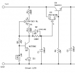
Some people prefer the hybrid NJFET+NPN Darlington topology. Instead of the standard Darlington with emitter follower driving emitter follower, it has a source follower driving an emitter follower. An example from the "SuperTeddy" regulator is attached. {BTW: notice the subtlety of resistor R6 -- usually it would be connected to the emitter of Q4 rather than to ground. Why has Teddy Pardo done it this way instead?} . On the other hand, a negative regulator needs a PJFET+PNP and PJFETs are pretty scarce these days. Toshiba's website lists exactly zero of them, for example.
If you decide to try the complementary feedback ("Sziklai") pair, you have no choice: you must build it from two discretes. Nobody sells integrated CFPs.
_
Attachments
Last edited:
Thanks. I need to do a lot of research/study before embarking. From what I've read so far the Sziklai configuration would have some advantages.
I'm still chewing on your question...I note that it is not uncommon for voltage regulators schematics to show the driver's emitter (source in this case) connected to ground via a resistor when the pass transistor is being driven by a collector.
Another perhaps interesting circuit is the Sparkos voltage regulator (link) with its 'bi-directional drive.'
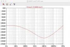
FWIW I dropped vsubthres parameter adjustment into the IPP037 model used in my LTspice model of this regulator (post 97). I made no attempt to question your value of 142m. As you note, adding the parameter makes the model better; whether it makes it 'good enough' I didn't take a view on. I merely wanted to see what impact such an adjustment had on the regulation circuit's predicted line rejection.
If - and that's a big if - the revised model is to be (more) believed, the circuit is still no slouch. I was rather worried it was going to turn into an absolute pig. Of course, as we've seen, there can be a great divide between LTspice prediction and an actual circuit's capability. But even if actual performance were to be a flat 120dB or so it would still be rather good. Not a Jung/Didden regulator, but still not bad.
I'm still chewing on your question...I note that it is not uncommon for voltage regulators schematics to show the driver's emitter (source in this case) connected to ground via a resistor when the pass transistor is being driven by a collector.
Another perhaps interesting circuit is the Sparkos voltage regulator (link) with its 'bi-directional drive.'
FWIW I dropped vsubthres parameter adjustment into the IPP037 model used in my LTspice model of this regulator (post 97). I made no attempt to question your value of 142m. As you note, adding the parameter makes the model better; whether it makes it 'good enough' I didn't take a view on. I merely wanted to see what impact such an adjustment had on the regulation circuit's predicted line rejection.
If - and that's a big if - the revised model is to be (more) believed, the circuit is still no slouch. I was rather worried it was going to turn into an absolute pig. Of course, as we've seen, there can be a great divide between LTspice prediction and an actual circuit's capability. But even if actual performance were to be a flat 120dB or so it would still be rather good. Not a Jung/Didden regulator, but still not bad.
Attachments
Sparkos's data sheet is refreshingly informative. The key to their "bi-directional drive" is the bias voltage source Vb. Imagine that it is implemented as a standard VBE multiplier circuit as used in audio power amplifiers. Imagine a crazy person is playing with the Vb circuit on the lab bench, slowly dialling a 25-turn trimmer potentiometer, looking for the resistance which gives Vb = 0.95 * (VBEnpn + VBEpnp). Or maybe 0.99 times. Or maybe whatever setting increases the total quiescent current by 500uA. Or ...
_
_
Attachments
If dBs of simulated line rejection is what you care about most, you can get at least 100 dB more (in LTSPICE!) by installing two or perhaps three LC filters upstream of the pass transistor. Since the output current is less than an ampere, the voltage drop across these filters will be nil, and the inductors will be small and inexpensive.But even if actual performance were to be a flat 120dB or so it would still be rather good. Not a Jung/Didden regulator, but still not bad.
Then you can get yet another 60 to 80 dB of line rejection in LTSPICE by installing keantoken's CFP capacitance multiplier (link) between the filters and the voltage regulator proper. Be sure to follow his recommendation to use a transistor with no quasi-saturation at all, like the BC327/BC337. Or use your Atlas Peak DCA Pro to draw the IV curves of other candidate transistors; the region you care about (sub 15 mA) is the region the Atlas occupies. The cap multiplier will cost you some voltage drop; I'd suggest you plan on 3V or so. Fortunately you can purchase the next step up in transformer secondary voltage, at no increase in cost and no danger of exceeding its VA capability. Instead of 15VAC secondaries, get 18VAC or 22VAC and squander that extra voltage by dropping it across a bunch of line rejection enhancing circuits all connected in cascade. Marvel at the 300dB attenuation in LTSPICE.
No, I was rather pondering just what might be the actual performance of the circuit I am using now in a couple of components. Very good - good - average - useless. I should take another look at measuring the supplies I have built. (I have assembled Sam Groner's low noise measurement amplifier and have dabbled a little with ARTA. And I now have a signal generator.)
Re Sziklai: I have an LTspice model up and running which replaces the IPP037 with a D44H11 driver and D45VH10 pass transistor. I'm still trying to get my head around sizing the resistor from emitter to base of the pass PNP transistor let alone anything more complicated.
EDIT: I suspect there are much better choices for the driver transistor given it is not having to deal with much current not Vce.
Last edited:
EDIT: I suspect there are much better choices for the driver transistor given it is not having to deal with much current nor Vce.
Maybe even something like a BC847C
A quick glance at Horowitz and Hill 3rd edition suggests it may be a good use of time to investigate the MMBT6429. Download its datasheet straight from ON Semiconductor's website and then study Figure 12 among others.
Thanks. I didn't have much time to spend on this today but I did drop in the MMBT6429 in lieu of the BC847C. It improved modelled line rejection a little. With regard to transistor speed or fT, isn't the circuit still constrained by the fT of the pass transistor? The pass transistor still needs to be able to react quickly to the changes in its base current inflicted by the driver...
I will try to spend more time on this tomorrow. I don't yet understand why a Darlington or Sziklai connection is 'slow' without a base-emitter resistor i.e. why Q1 can't turn off Q2 quickly (even if the driver Q1 is very 'fast'). The discussion in Horowitz and Hill where these two connections are introduced states the condition without explanation.
I will try to spend more time on this tomorrow. I don't yet understand why a Darlington or Sziklai connection is 'slow' without a base-emitter resistor i.e. why Q1 can't turn off Q2 quickly (even if the driver Q1 is very 'fast'). The discussion in Horowitz and Hill where these two connections are introduced states the condition without explanation.
You will enjoy finding solutions to these and other design problems as you proceed.
H&H are using the words "turn Q2 on" to mean "charge Q2's base-emitter capacitance" . Similarly they are using the words "turn Q2 off" to mean "discharge Q2's base-emitter capacitance". The diffusion portion of this capacitance (which is the dominant portion) is linearly proportional to the emitter current. And emitter current equals collector current if beta is high, so these lecture notes I just grabbed from Georgia Tech's website, talk about Ic rather than Ie. A transistor carrying a lot of current is difficult to "turn on" or "turn off" because its base-emitter capacitance is quite large. H&H are telling you it takes a lot of current to charge and discharge the (surprisingly large) base-emitter capacitance if you want to do it quickly.
See if your calculator gets the same answer as mine: a 50 MHz transistor like the D45H11 (tauF = 1/(2*pi*fT) = 3.18 nsec), carrying Ic = 1 ampere, has a base-emitter capacitance of 0.12 microfarads. That's 120,000 picofarads!! ("VT" in the figure stands for the "thermal voltage," namely (kT/q), which equals 0.026 volts at room temperature).
_
Attachments
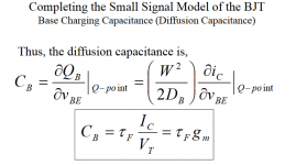
The diffusion portion of this capacitance (which is the dominant portion) is linearly proportional to the emitter current. And emitter current equals collector current if beta is high
_
Thanks. This is the bit I didn't appreciate. I could not understand why the discharging of base-emitter capacitance was such an issue for a Darlington or Sziklai connection and not for a regular BJT pass transistor situation. Is it also the case that with the Sziklai (for example) where an NPN collector drives a PNP pass transistor, turning off the PNP involves charging the base-emitter capacitance of the PNP pass transistor, yet the driver collector can only sink current from the pass transistor base?
Last edited:
SPICE gives the right answer in this particular case. When the load current drawn from the regulator suddenly steps from 1.0 ampere to 0.05 amperes with a fall time of 20 nanoseconds, the behavior of the base current(s) in the output stage transistor(s) as reported by SPICE, is correct (I claim). Same goes for the other edge of the square wave, when load current suddenly steps from 0.05 amperes to 1.0 amperes in 20 nsec.
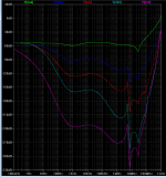
Here's ~ 210 dB of additional LTSPICE line rejection, before your regulator.
It occurred to me that what you are probably seeking before your regulator, is to get a whole lot of line rejection at very low frequencies, too low for bypass capacitors. Too low for inductor/capacitor filters. Get rid of ripple and of infrasonic signals, just present a nice pure DC input to your Super Regulator.
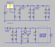
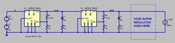
It looks like the TI LM2941 low dropout voltage regulator IC fits the bill. It's output current meets your spec (>1 amp), while having a surprisingly low dropout voltage (0.5V). The number of discrete parts per stage of regulation is very small: only five parts! (six if you count the heatsink). So you can cascade more than one stage of regulation without dropping a lot of voltage and without clogging your board with massive numbers of parts.
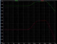
TI gives away an "Unencrypted PSPICE simulation model" of the LM2941, which appears to work jolly well in LTSPICE. I cascaded two of them and got 150 dB of line rejection at 0.1 Hertz (!). Inductors and capacitors and capacitance multipliers even with Keantoken's Sziklai topology can't possibly do that. Schematic and line rejection simulated results are attached below.
_
Attachments
Interesting. I dropped one set of these into the Sziklai circuit shown in the link above (post 118), just after the second 1,000uF input cap (and ahead of the current source). For some reason the Sziklai pass transistor configuration after it no longer works. I haven't figured out why yet. Without the LM2941 the Sziklai works fine. The LM2941 alone works fine. Couple them together and they don't. I suspect it is something to do with the way the LM2941 ramps up.
(A pre-reg like this has the added benefit of saving me having to think about a current regulator.)
(A pre-reg like this has the added benefit of saving me having to think about a current regulator.)
Last edited:
- Status
- Not open for further replies.
- Home
- Amplifiers
- Power Supplies
- Thermal considerations for Fairchild SDIP bridge rectifiers