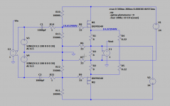
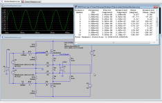
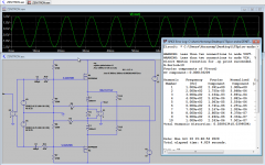
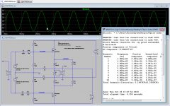
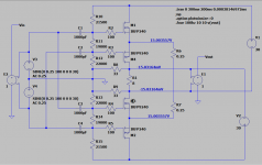
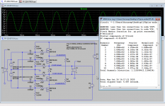
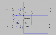
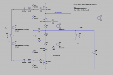
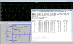
The inductor is there to break up the feedback loop that otherwise turn the devices into source followers. It creates voltage gain.
It is a SoZ V.7 with super symmetry feedback from the alternative Circlotron universe, where you don't need the bottom CCS or high power resistors.
The schematic posted above is just taken from my rather hazy memories from when I built that amp.
It is not optimized in any way. I would definitely want to spend some quality time in LTSpice before committing to real devices, power supplies and heat sinks.
Last edited:
any advantage compared to a common source circlotron that don't need the inductor to have some gain?
common source circlotron that don't need the inductor to have some gain?
How do you design a single stage circlotron without inductors or signal transformers that does have voltage gain?
Can you show the same for the version with the inductor load? How much voltage gain do you get with the inductor load?
(I have to admit that I don't quite get how/why the inductor or resistor causes any voltage gain, but I am sure I'll figure it out somehow.)
(I have to admit that I don't quite get how/why the inductor or resistor causes any voltage gain, but I am sure I'll figure it out somehow.)
How do you design a single stage circlotron without inductors or signal transformers that does have voltage gain?
indeed with one stage I understand it is impossible because there is no common reference for both gates, therefore a signal transformer is needed at the input.
But with 2 stages it is the amazing fet circlotron
Build The Amazing FET Circlotron | Pass DIY
how both compare?
still dominant 3rd harmonic?
But with 2 stages it is the amazing fet circlotron
I came up with that design a few years before it was published at the Passdiy site.
I have never had the chance to compare them side by side. Both should be third harmonic dominant since both are balanced and has some second harmonic cancellation mechanism inherent in the design.
The Zenitron amp design was my try at making a simple one stage circlotron with voltage gain.
It was many years since I last had a listen to the Zenitron design. I have scavenged my ugly rats nest build for parts, but I would like to build a new Zenitron based on a matched pair of IXYS IXTH16N20D2 depletion mode devices to simplify the bias circuitry and the super symmetric feedback.
IXYS IXTH16N20D2
Why this part?
What does it take to drive the inputs of the Zenitron? Does it need a source with a low-impedance output?
Biasing the Depletion Mosfet
The difficulty with Circlomanen's circuit above is getting matched inductors with the right DCR to bias the depletion mosfets. Apart from that, a very simple circuit which I like a lot.
The difficulty with Circlomanen's circuit above is getting matched inductors with the right DCR to bias the depletion mosfets. Apart from that, a very simple circuit which I like a lot.
Why this part?
It is a depletion mode device with a usable Vgs of approximately -2 volts for 2 ampere of quiescent current.
See Nelson Pass article The De-Light amplifier for more information about depletion mode devices. http://www.firstwatt.com/pdf/art_delite.pdf
getting matched inductors with the right DCR to bias the depletion mosfets
A large transformer core with bifilar windings and 0.5 to 1.5 Ohm resistance is usable. I would guess that 1.0 Ohm resistance is quite optimal for those devices.
You could wind 2 parallel 150 meter strands of 2.5 mm coupling cable around a massive piece of steel or several layers of stacked flat bar.
See Solhagas excellent build of SLAPS for Bass and SLAPS for SLAM for examples of easy to build inductors. It is easy to increase the inductance substantially by using a closed magnetic circuit.
https://www.diyaudio.com/forums/solid-state/346879-slaps-bass.html?highlight=SLAPS
https://www.diyaudio.com/forums/solid-state/343903-slaps-slam.html?highlight=SLAPS
Why not use a current source ?
How much extra voltage would it need ?
Something like 5V ?
Can we not use the same depletion devices as current source, e.g. the matching rejects ?
Cheers,
Patrick
How much extra voltage would it need ?
Something like 5V ?
Can we not use the same depletion devices as current source, e.g. the matching rejects ?
Cheers,
Patrick
Last edited:
The input impedance can be set to other values dependent on the devices, the intended frequency range and what kind of preamp you have.
The IXTK16N20D2 does have a rather hefty gate capacitance and I would guess they need quite low resistance in series with their gates to avoid excessive distortion in the high frequency range.
It is possible to use constant current sources or modulated current sources instead of a large bifilar winded coil. The CCS would need at least as much voltage as the active devices, which kind of detracts from the simplicity and efficiency of the design.
The Zenitron is a Zv7-T http://www.firstwatt.com/pdf/art_zv7.pdf but "circlotronified" to avoid the bottom CCS and the input capacitors of that design.
What Nelson Pass writes in the Zv7 article applies to this design, with the exception of the bottom CCS.
Just for the sake of technical discussion.
Let's take your circuit in #111.
Assume we bias at say 1.2A, the IXTH16N20 needs a Vgs of ~ -2.4V.
So this is what the CCS has as total headroom, while inputs can still be DC coupled.
We can take a IXTH20N50, which needs almost no source degeneration for 1.2A.
So the entire 2.4V can be used as Vds, which is sufficient according to datasheet.
And then of course the mid-point of the speaker (or the 2x 33R) does not have to sit at Gnd.
It can be at a constant negative voltage, and the CCS will get more headroom.
And 2x depletion NMOS is for me simpler than winding inductors.
Hopefully I have not missed anything really stupid without thinking it through thoroughly,
Patrick
As to the high capacitances of the 16N20, one solution can be to use another 16N20 as self-biasing cascode.
The lower (driver) NMOS will then get a nearly constant 2.4V Vds, which also looks OK from datasheet.
So 6x 16N20 in total per circlotron.
Patrick
The lower (driver) NMOS will then get a nearly constant 2.4V Vds, which also looks OK from datasheet.
So 6x 16N20 in total per circlotron.
Patrick
- Home
- Amplifiers
- Pass Labs
- The Zenitron
