... should have.... but the Rm is at least 5x higher so that the power used must be at least 5x lower!
True, since the ESR for a 3rd overtone 11.2896 MHz Sc-Cut crystal is around 100 ohm, the jfet cannot drive it, because it has not enough transconductance. But it has a Q around 1M, while the AT-cut type at the same frequency is 150K.
The Driscoll oscillator, using a bjt with enough gain, can drive it.
The Driscoll oscillator, using a bjt with enough gain, can drive it.
I have no good experiances with the Driscoll....
I have no good experiances with the Driscoll....
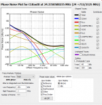
Theoretically the Driscoll oscillator should be the best way to get low phase noise close to the carrier, since it provides very high loaded Q. Simulating the circuit with a 11.2896 MHz SC-Cut 3rd overtone crystal, Q around 800K, the loaded Q is 91.7%, or 733K, with 77uW drive level. The in-circuit losses are minimal, since the crystal sees a very low impedance.
Moreover, the crystal has direct emitter control of the transistor’s gain. Also, the crystal is located at the lowest power point in the circuit, and the output is taken at the highest amplitude point, with maximum signal to noise ratio.
Hello Andrea (and Herbert) and thank you for your wonderfull efforts and cooperation.
BTW... do you have the possibilty to perform PN measurements on the Driscoll oscillator you have built?
Best wishes
BTW... do you have the possibilty to perform PN measurements on the Driscoll oscillator you have built?
Best wishes
Hello Andrea (and Herbert) and thank you for your wonderfull efforts and cooperation.
BTW... do you have the possibilty to perform PN measurements on the Driscoll oscillator you have built?
Best wishes
As I said in first post I have limited access to a university lab to use an Agilent E5052 to measure the phase noise.
As soon as all the 3 oscillators (Clapp, Driscoll and Butler) will be ready I'll go to the lab to measure their performance.
As I said in first post I have limited access to a university lab to use an Agilent E5052 to measure the phase noise.
As soon as all the 3 oscillators (Clapp, Driscoll and Butler) will be ready I'll go to the lab to measure their performance.
***************************************************
Hello Andrea and thanks for the feedback.
Best wishes.
Last edited:
Theoretically the Driscoll oscillator should be the best way to get low phase noise close to the carrier,..................., and the output is taken at the highest amplitude point, with maximum signal to noise ratio.
Oh yes, it is all true in theory but did you build the oscillator and measure the close-in noise?
Better to keep clock rate low?
Many oscillators show higher phase noise at low Hz, and some families show higher low Hz phase noise as the freq goes up. Consider a DSD DAC clock where 22 Mhz is roughly DSD512. Does this mean that if we use a 45 Mhz clock, the low Hz phase noise necessarily is higher? What is the best way to divide the clock rate in order to maintain the lowest phase noise, this needs to be software controlled because the DAC needs to deal with DSD 64,128,256,512 and possibly 1024.
Many oscillators show higher phase noise at low Hz, and some families show higher low Hz phase noise as the freq goes up. Consider a DSD DAC clock where 22 Mhz is roughly DSD512. Does this mean that if we use a 45 Mhz clock, the low Hz phase noise necessarily is higher? What is the best way to divide the clock rate in order to maintain the lowest phase noise, this needs to be software controlled because the DAC needs to deal with DSD 64,128,256,512 and possibly 1024.
............, and some families show higher low Hz phase noise as the freq goes up.
Each doubling in frequency enlarges the (close-in) phase noise with 6 dB! This is a phisical law and is independant of the type of oscillator. I do not understand why one should want DSD 128, DSD 256 etc. Above DSD 64 is no quality gain any more, so stay with 11.2.... MHz.
I say it again: I have the experiance that the power in the resonator is the most important factor for low phase noise. What could the Q do at a distance from the carrier of 10 Hz? Nothing! A low Rm is important to make it possible that a high HF-current can be allowed in the Xtal.
Herbert.
Last edited:
Each doubling in frequency enlarges the (close-in) phase noise with 6 dB! This is a phisical law. I do not understand why one should use DSD 128, DSD 256 etc. Above DSD 64 is no gain any more.
Would it be possible to use a clock recovery PLL circuit to reduce phase noise?
Would it be possible to use a clock recovery PLL circuit to reduce phase noise?
A PLL circuit should be avoided in any case!!! Work asynchronous if possible.
Herbert.
A PLL circuit should be avoided in any case!!! Work asynchronous if possible.
Herbert.
LMK04828 | Dual / Cascaded PLL | Clock Jitter Cleaners | Description & parametrics, My understanding is that these have been developed for phased array radar applications and are considered to perform well at high frequencies but I do not claim to be an expert. 91 fs RMS jitter at 100hz -- what is the catch?
Trying to learn.
Those are interesting enough to give the tool a try. Unfortunately it won't work.
I used the tool and it needs a VCXO at around 500 MHz??? and won't come out with the right frequency even going in with it. I'm sure it can be configured but its not lots better in phase noise or jitter than a good crystal oscillator. And its way harder to use. (BGA anyone?)
Those really low numbers aren't that low when the fundamental is 2.4 Ghz. The period is 400 pS so it must be in the fS or its not useful.
Attachments
91 fs RMS jitter at 100hz -- what is the catch?
Trying to learn.
Here we are talking about 100 fs. That is <130dBc@10 Hz.....
Herbert.
Last edited:
A PLL circuit should be avoided in any case!!! Work asynchronous if possible.
Herbert.
If you can, a VCXO with a good PLL to lock to the incoming clock is ideal but hard to implement in systems where the sample rates can change all the time.
a VCXO with a good PLL to lock to the incoming clock is ideal.
A VCXO is always worse than an XO...!!!
Herbert.
Hi again ... I have a question that I hope maybe Herbert, Gerhard, Alexiss, Andrea & 1audio could take an interest in elaborating on ... as it is 1audio already gave fine feedback on this some time ago but I've just been wondering if there might be other solutions ...
As it is most audio systems have both 44.1 & 48 kHz based oscillators which means that there needs be a way to switch between these two frequency bases. Also, if I remember correctly Andrea (?) earlier in the thread mentioned that having the individual oscillator on for some time improves the oscillator's jitter/phase noise. To this end 1audio (Demian) earlier suggested: "you can either use some nand gates to switch as well as buffer or add a CMOS mux to switch between oscillators" This sounds like good advice, however, since such a "switch" is directly in the oscillator path I was wondering if there may be some "complementary" approaches to this switching ... ? Maybe a preferred MUX or NAND gate ... ?
... 🙂 Spring is approaching 😉 ...
Cheers,
Jesper
earlier suggested: "you can either use some nand gates to switch as well as buffer or add a CMOS mux to switch between oscillators" This sounds like good advice, however, since such a "switch" is directly in the oscillator path I was wondering if there may be some "complementary" approaches to this switching ... ? Maybe a preferred MUX or NAND gate ... ?
You must build two separate oscillators completed with a slicer (74HC04). Thereafter you could switch from the one oscillator to the other
Herbert.
You must build two separate oscillators completed with a slicer (74HC04). Thereafter you could switch from the one oscillator to the other
Herbert.
Hi Herbert,
Thanks for your feedback ... This was actually what I was intending to do, however, since the NAND gate or MUX will be directly in the "clock-path" I was wondering if the NAND gate (or a particular NAND gate?) would be the best solution ... ? Since there's been some discussion here about the various slicer IC options I assumed something similar could be the case with a switch - be it a NAND gate or a MUX of some kind ...
Well, have a good evening to those reading ;-)
Jesper
Hi Herbert,
or MUX will be directly in the "clock-path" I was wondering if ..... would be the best solution ... ?
I'm investigating this for TentLabs but got already the idea that a MUX in the clock-path does not do any harm...
H.
- Status
- Not open for further replies.
- Home
- Source & Line
- Digital Line Level
- The Well Tempered Master Clock - Building a low phase noise/jitter crystal oscillator