Since there is not a standard I2S connection I would avoid to provide a connection for a specific device.
There is a 10 pin connector on the board and I will provide an assembled cable not termitated at one side, so one can connect whatever device.
The price has not yet been defined, but there will be 3 options:
- bare board, all the parts to be assembled
- semi finished board, users have to solder a few parts (cheaper solution)
- finished board, all parts assembled and tested (most expensive solution)
but how can we do reclocking LE prior to PCM63 In that case
I believe that the SM5842 does not manage I2S, so you should put the FIFO buffer before the SM5842.
There is no way, you should remove the SM5842 and do the oversampling via software before feeding the FIFO.
To get the FIFO buffer to feed directly the PCM63 you have to convert the output of the SM5842 to I2S format, but I don't know if such that converter is available.
To get the FIFO buffer to feed directly the PCM63 you have to convert the output of the SM5842 to I2S format, but I don't know if such that converter is available.
Yes, it's possible.
Firstly you should measure the voltage at pin 27 with a DMM to understand the mode select configuration.
Then you should remove the CS8414 and feed directly the TDA1541A by I2S or PCM simultaneous depending on the actual mode select configuration.
The TDA I2S pins are 1,2,3 and 1,2,3,4 in simultaneous mode.
I see 3 jumpers on the PCB (R9, R10, R11), maybe they are connected to the I2S input of the TDA, you should look at the bottom of the PCB to understand where they are connected. If they are connected to the I2S input of the TDA1541A (pins 1,2,2) you should simply cut the jumpers and connect the incoming I2S signals to the right side of the jumper.
Thank you very much Andrea!! Seems a bit complicated 🙂(
would you please recommend optimal reclocking setup for cs8412 sm5842 pcm63 based dac
I think you also got that set time ago
I think you also got that set time ago
There is no way, you should remove the SM5842 and do the oversampling via software before feeding the FIFO.
To get the FIFO buffer to feed directly the PCM63 you have to convert the output of the SM5842 to I2S format, but I don't know if such that converter is available.
@jmmbarco
It's not so complicated, maybe Mr. Abbas can help you to understand what you have to tweak.
It's not so complicated, maybe Mr. Abbas can help you to understand what you have to tweak.
would you please recommend optimal reclocking setup for cs8412 sm5842 pcm63 based dac
I think you also got that set time ago
I think the only way is FIFO-SM5842-PCM63, but I believe you could achieve better performance removing the 5842 to feed directly the PCM63 from the FIFO reclocker.
Hi Andrea,
As other member suggested, would you at least consider implement LT3045 for supply OCXO? This would definitely improve the sound quality.
As for MCU and CPLD, I think you can preserve some space for 3-terminal regulator like LM7805, because this won't take much space, and users can use LM7805-compatible LT3045 regulator modules if they want, isn't it great?
There seem to be isolator on the board, can you please consider using NVE IL715 series? They have better performance and lower jitter compared to TI's ISO or AD' ADuM series.
By the way, when do you plan to release your product to the community, any schedule? I am anticipating your product.
Regards,
Eric
Forgot to say.
About the display. Can you consider OLED or LCD?
2 reasons.
1. A OLED display module can provide more information, makes UI more friendly. Sample rate, Input Source, Word Clock, etc. can be shown on the screen at the same time.
2. More importantly, a long square monitor like OLED is easier for DIYer to drill the hole and fixation is easier to.
For LED block, DIYer have to locate them precisely and make MORE square holes to fix the LED.
I would sincerely and strongly suggest you to consider OLED or even VFD module. OLED is not expensive, and provides much more advantages; Color TFT is also good, it can display information on differed colors.
Please, Please, think about OLED!!! Thank you 🙂
There are many inexpensive and good quality VFD ore OLED monitor on market.
Samsung and Japanese Noritake have quite nice VFD, using SPI or serial protocol.
It would really really be awesome if the monitor is OLED/VFD.


Samsung and Japanese Noritake have quite nice VFD, using SPI or serial protocol.
It would really really be awesome if the monitor is OLED/VFD.
There are many inexpensive and good quality VFD ore OLED monitor on market.
Samsung and Japanese Noritake have quite nice VFD, using SPI or serial protocol.
It would really really be awesome if the monitor is OLED/VFD.
View attachment 880771
View attachment 880772
View attachment 880774
We suggest external oscillators for the FIFO board, so they have separate power supply, preferably battery.
MCU and FPGA have their power supply on board, no need of stellar regulators here since they are isolated from the I2S output.
Digital isolators have anyway bad jitter performance but we don't care about since the crucial signals come directly from the master clock via copper.
That's the reason we have chosen optical isolators, they are a truly brick wall against EMI/RFI.
Sorry but an OLED display needs RF to work and we would avoid any interference from other devices, so we cannot implement such user interface.
During the listening the MCU is in stand by mode to avoid any RF generation, the display are refreshed only if a parameter changes (sample rate, dithering).
This way doesn't work with OLED display.
There is a price to pay to get the better audio performance.
Thanks for explanation, very nice job!
Maybe another suggestion: can you consider to make gold-plated PCBs for massive-production version?
I am so excited to see the product, may I ask your time schedule? Would this project be released within maybe one month? or maybe 2 months?
would you please recommend optimal reclocking setup for cs8412 sm5842 pcm63 based dac
I think you also got that set time ago
For the recklocking You need 2x clock then data. That is at least 2X BCK Fr
use cascade Flip-Flop for each line to preserve one full clock "delay" and rising / falling edges like they was before recklocking
cheers
if You want for reckock to be working with higher SR like 384KHz choose interfaces with 44/48MHz oscilators or master clocks.
Yes, it's possible.
Firstly you should measure the voltage at pin 27 with a DMM to understand the mode select configuration.
Then you should remove the CS8414 and feed directly the TDA1541A by I2S or PCM simultaneous depending on the actual mode select configuration.
The TDA I2S pins are 1,2,3 and 1,2,3,4 in simultaneous mode.
I see 3 jumpers on the PCB (R9, R10, R11), maybe they are connected to the I2S input of the TDA, you should look at the bottom of the PCB to understand where they are connected. If they are connected to the I2S input of the TDA1541A (pins 1,2,2) you should simply cut the jumpers and connect the incoming I2S signals to the right side of the jumper.
@jmmbarco
If It possible to obtain Time simoultaneous format , my tip is to cut the trace from format selection pin (if it is on I2S format selected) AND rearrange selection and inputs like Andea said, to Time simultaneous format - much better sounding tda1541A (for my ears...)
Last edited:
Hi Andrea and Zoran!,
Since my last post I have been investigating about Andrea´s suggestion.
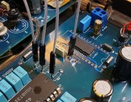
Actually these 3 jumpers next to the TDA socket (R9, R10, R11) are the incoming I2S signals from the CS8414 (fantastic intuition Andrea!!). I have found a diyer at dastereo.ru who has already carried out this mod. Just look at the first attached picture.
What can be seen in the picture are the I2S output lines coming from Pi2Design 502DAC as well as Allo Kali reclocker (pictures 2 and 3). I have compared the photos with the kali pinout and 3 front lines pin connections corresponds to BCLK (pin12) + LRCLK (pin 35) + DATA (pin40) and GND(pin39) is the back line. MCLK is not used.
As no further tweaks are performed, I assume that input data format must be I2S – MUX TWC and not OB, am I right? If that´s the case, one first mod could be, as Andrea suggested, just cutting these the jumpers and connect the direct I2S signals as in the first photo.
What I have thought is installing Andrea´s FIFO inside Abbas DAC and connecting:
1. FIFO output to the right side of the jumper (soldered).
2. Left side of the jumper (CS8414 I2S output) to a free FIFO input. Input #4 would be better as I should need a shorter connection. Doing so, I could keep full DAC functionality!
3. External I2S signal coming from my digital audio transport to a free FIFO input. Input #1.
4. FIFO psu would be probably installed inside Abbas DAC as well.
5. FIFO Master Clocks (Driscolls 5/6) and FDs would be in a separate box, connected via SMA cable.
However, I have many doubts that makes me feel unsure about final result. For example. Abbas DAC implements a quite unique tube DEM clock for the TDA and I don´t know if this could affect to the mod or DEM performance. I think that it does not but I am not sure.
As Zoran suggests, going to simultaneous mode would double the max SR, and I could get 384kbps but I am not sure wether the whole DAC design would benefit from this SR. Actually, there is no jumper for pin4 and I should probably mod pin27 as well. My “high-SR days” passed away and I really think that “going slow” can be the way to get best SQ. DAC sounds so beautifully now that I am really scared to ruin its magic lifeness. I would never consider modding it If I didn´t think that the Andrea´s products line is truly SOTA and could take the most out of my DAC. Probably Zoran mod would be the way even keeping 96khz SR, but it is more complicated and uncertain, so I am not at all sure of what to do. I have attached a photo of my beloved DAC (ugraded v3.1: pic #4).
Although it seems feasible, it is probably beyond my hand soldering skills, but I could ask for help and do the trick. I will contact Mr. Abbas as well before doing anything.
What do you think guys?? Thank you very much in advance!!!
Best,
JM
Since my last post I have been investigating about Andrea´s suggestion.
Actually these 3 jumpers next to the TDA socket (R9, R10, R11) are the incoming I2S signals from the CS8414 (fantastic intuition Andrea!!). I have found a diyer at dastereo.ru who has already carried out this mod. Just look at the first attached picture.
What can be seen in the picture are the I2S output lines coming from Pi2Design 502DAC as well as Allo Kali reclocker (pictures 2 and 3). I have compared the photos with the kali pinout and 3 front lines pin connections corresponds to BCLK (pin12) + LRCLK (pin 35) + DATA (pin40) and GND(pin39) is the back line. MCLK is not used.
As no further tweaks are performed, I assume that input data format must be I2S – MUX TWC and not OB, am I right? If that´s the case, one first mod could be, as Andrea suggested, just cutting these the jumpers and connect the direct I2S signals as in the first photo.
What I have thought is installing Andrea´s FIFO inside Abbas DAC and connecting:
1. FIFO output to the right side of the jumper (soldered).
2. Left side of the jumper (CS8414 I2S output) to a free FIFO input. Input #4 would be better as I should need a shorter connection. Doing so, I could keep full DAC functionality!
3. External I2S signal coming from my digital audio transport to a free FIFO input. Input #1.
4. FIFO psu would be probably installed inside Abbas DAC as well.
5. FIFO Master Clocks (Driscolls 5/6) and FDs would be in a separate box, connected via SMA cable.
However, I have many doubts that makes me feel unsure about final result. For example. Abbas DAC implements a quite unique tube DEM clock for the TDA and I don´t know if this could affect to the mod or DEM performance. I think that it does not but I am not sure.
As Zoran suggests, going to simultaneous mode would double the max SR, and I could get 384kbps but I am not sure wether the whole DAC design would benefit from this SR. Actually, there is no jumper for pin4 and I should probably mod pin27 as well. My “high-SR days” passed away and I really think that “going slow” can be the way to get best SQ. DAC sounds so beautifully now that I am really scared to ruin its magic lifeness. I would never consider modding it If I didn´t think that the Andrea´s products line is truly SOTA and could take the most out of my DAC. Probably Zoran mod would be the way even keeping 96khz SR, but it is more complicated and uncertain, so I am not at all sure of what to do. I have attached a photo of my beloved DAC (ugraded v3.1: pic #4).
Although it seems feasible, it is probably beyond my hand soldering skills, but I could ask for help and do the trick. I will contact Mr. Abbas as well before doing anything.
What do you think guys?? Thank you very much in advance!!!
Best,
JM
Attachments


Last edited:
Yes Abas dac using DEM but i think with sine vawe frequency not squared vawe. And he have tube version of DEM oscilator.
in all input format modes this DEM modul remains in the dac circuit.
I am not sure about TDA1541A can go up to 384KHz NOS mode? Probably can? I cant remember now about my test of TDA1541A... Sorry...
I tested TDA1540 and I can confirm that it can go up to 384KHz. BUT the specifications tells that TDA1540 is 12MBit/sec speed
and for TDA1541A is stated 6Mbit/sec (probably because of higher density for 2 dac in the DIE?
Last edited:
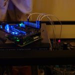
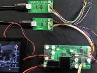
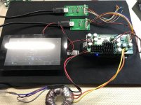
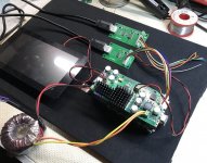
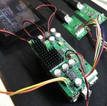
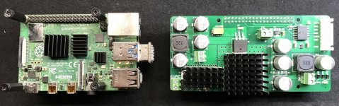
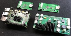
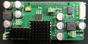
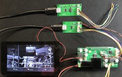
Since we are planning to implement a Raspberry as a standalone source for our audio system, we have developed a few boards to interface it with our new FIFO.
The source includes the Raspberry PI, the 7" touch screen and an expansion boards to connect a SSD.
The SSD expansion board is stacked under the RPI.
The first board (TWSAFB-RPI) is an interface to the Raspberry and it's stacked onto the RPI. It provides power supply for the RPI and the Touch screen, and also a rail to supply the I2S transmitter. The I2S output is isolated from the Raspberry.
The second board (TWSAFB-TX) is the I2S LVDS transmitter powered by the TWSAFB-RPI.
The third board (TWSAFB-RX) is the I2S LVDS receiver to be placed far from the Raspberry and close to the FIFO. Its I2S output is isolated from the trasmitter to avoid any EMI/RFI interference. The input part of the receiver is powered by the transmitter, while the isolated output has to be powered by the FIFO.
An ordinary HDMI cable is used to connect the transmitter to the receiver.
The Raspberry power supply and interface board TWSAFB-RPI is ready and tested succesfully.
I attach a few pictures with the whole parts of the standalone RPI source.
Attachments
-
 TWSAFB-RPI_03.JPG232.8 KB · Views: 399
 -
 TWSAFB-RPI_05.JPG160.5 KB · Views: 408
 -
 TWSAFB-RPI_06.JPG139.6 KB · Views: 400
 -
 TWSAFB-RPI_07.JPG128.2 KB · Views: 388
 -
 TWSAFB-RPI_09.JPG174.9 KB · Views: 351
 -
 TWSAFB-RPI_11.JPG143.6 KB · Views: 358
 -
 TWSAFB-RPI_10.JPG166.5 KB · Views: 417
 -
 TWSAFB-RPI_13.JPG170.1 KB · Views: 452
 -
 TWSAFB-RPI_14.JPG213.2 KB · Views: 737
 -
 TWSAFB-RPI_01.JPG296.2 KB · Views: 427
- Home
- Source & Line
- Digital Line Level
- The Well synchronized asynchronous FIFO buffer - Slaved I2S reclocker