Indeed the metal can is probably worth the extra money, Mouser has the metal package for $13 bucks or so.
The 14pin dip is worth it just for the voltage reference alone.
The 14pin dip is worth it just for the voltage reference alone.
Ive used the Maida in a few supplies using the EL34 for a pass element, it made a nice power supply.
Yes the metal can differs in price wildly between vendors, and it has a few versions with a range of specs as well which affects the price.
Referring to the schematic in post #51 and the value of R20 (marked USER) for the HV regulator, the following resistor values are listed with details on the HV DC output voltage range. This is based on R21 being 250 ohm giving an adjustment pin current of 5mA for the LM317 which has an internal Vref of 1.25VDC,
With trimpot RV3 having a value of 10K (single or multi turn) the pot dissipation will be a max of 0.25watts if the wiper is sitting at the HV GND point with 50VDC across the pot. Then R20 will give the following:
R20 = 22K 3W - output HVDC range will be 110 to 160V
R20 = 27K 3W - output HVDC range will be 135 to 185V
R20 = 33K 3W - output HVDC range will be 165 to 215V
R20 = 39K 3W - output HVDC range will be 195 to 245V
R20 = 47K 3W - output HVDC range will be 235 to 285V
With trimpot RV3 having a value of 15K ( single or multiturn) the pot dissipation will be a max of 0.375watts if the wiper is sitting at the HV GND point with 75VDC across the pot. Then R20 will give the following:
R20 = 22K 3W - output HVDC range will be 110 to 185V
R20 = 27K 3W - output HVDC range will be 135 to 210V
R20 = 33K 3W - output HVDC range will be 165 to 240V
R20 = 39K 3W - output HVDC range will be 195 to 270V
R20 = 47K 3W - output HVDC range will be 235 to 310V
Just a note on trimpots, most have a dissipation max of 0.5W, however the TT Electronics 93P series single turn has a max dissipation of 1W. Also the 15 K value is only available in a limited number of Bourns types. I will use the 10K 93P type as I have had very good experience with them in my past working life when they were originally introduced by Beckman in the US. and they have the slightly higher ratings. Of course if you select the value of R20 so that the pot will be adjusted roughly mid way for the required output regulated HVDC, then the pot dissipation will be half of the max stated above.
Working backwards, the HV regulator should have an input voltage of at least 25VDC higher than the required output voltage, then add the volt drop across any CRC or CLC after the rectifier bridge - then divide that sum by 1.4 for a full wave rectifier to give the required transformer secondary voltage.
I hope that is clear for all contemplating a build.
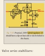
I have built multiple power supplies using this principe, but not with 7805 and zeners.I have Merlin Blencowes book on power supplies, and here is an intresting hybrid using the 7805.
Beware that the silicon sees the entire grid-cathode potential of the pass tube, thats why LM317HV is much better here, TL783 is much better than a 317 or 7805 but it requires a minimum output load of 15mA to remain stable.
One workaround is the LR8 IC with a PNP like MJE350 over it to increase the current capability of the IC. Ive tested this and it works really well.
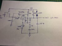
Attached my hand drawn schematic. Im using the pass tubes heaters to create a +17V supply with respect of the output which is RC filtered an fed to G1 of the pass tube.
Cout is 1uF minimum to maintain stability.
Attachments
Last edited:

I think you will find we will have the LR8 covered as well, stay tuned.
Only problem is its availability at the moment.
Only problem is its availability at the moment.
Gary and I are going over the BOM and finalization of what we hope will be pleasing to everyone for our LM317 version of the PSU. As mentioned by Gary we'll be cranking out an LR8 variant as well. Tentatively perhaps a 723 version but no promises there.
As far as the trimpots are concerned, when selecting parts I found that there's a fairly wide variety of footprint arrangements on top of existing part shortages making availability of parts increasingly difficult. I decided to come up with a footprint that would fit a decent variety of trimpots as we have the space on the board. Both low voltage and high voltage trimpots are utilizing this footprint at this time. Take a look at the image below, I hope that it makes sense to everyone. The second image shows a quick snippet example of different trimpot footprints. With a simple 3x3 grid of pins that are (I hope) well labeled, I think a wide variety of trimpots are accommodated. Pin pitch is 2.54mm.


As far as the trimpots are concerned, when selecting parts I found that there's a fairly wide variety of footprint arrangements on top of existing part shortages making availability of parts increasingly difficult. I decided to come up with a footprint that would fit a decent variety of trimpots as we have the space on the board. Both low voltage and high voltage trimpots are utilizing this footprint at this time. Take a look at the image below, I hope that it makes sense to everyone. The second image shows a quick snippet example of different trimpot footprints. With a simple 3x3 grid of pins that are (I hope) well labeled, I think a wide variety of trimpots are accommodated. Pin pitch is 2.54mm.
Bh is doing a mighty job on this versatile PSU, just to point out the value of R20 as shown in post #65 for the HVDC output adjust range - will now refer to R19 when Bh posts the updated schematic.
Everyone, gary s and I are proud to present what I've now dubbed the A.E.R.A.T.O.R. v1.1-LM317 (AdjustablE RegulAted Tube pOweR).
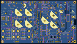
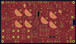
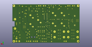
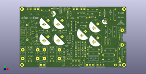
I will be updating the first post soon enough, but here is the v1.1 schematic, BOM, board layout, top and bottom tracks, and 3d renderings.
At this time I have not posted the gerbers themselves but will happily post them if people request it. I am happy to be the guinea pig for initial testing and will be placing an order shortly with JLCPCB for a set of 5 boards, 1.6mm thick with 2oz copper. When the board is tested and validated as good, I'll get to work on our LR8 based version. Though I am confident in the LM317 board, the one place I am not certain is the MIC29153/303/503 LDO models and the error flag pin. This is elaborated on further below, but let's talk about the board itself.
The Board:
Dimensions are 182mm long by 104mm wide. Given current potentials in the low voltage section it is strongly advised for 2oz copper weight.
High Voltage:
High voltage input accepts single/parallel secondaries, center tapped transformers, and even tube rectifiers. The BOM notates which parts to omit depending on your high voltage needs. Users can use this as a CLC with an off board choke via L1 and L2 terminals on J9, or a CRC by populating R13, this does require the user calculate R13 value and power rating per output voltage needs. This feeds an LM317 based high voltage regulator that is capable of a wide range of output voltages.
With R16 (marked USER) for the HV regulator, the following resistor values are listed with details on the HV DC output voltage range. This is based on R19 being 250 ohm giving an adjustment pin current of 5mA for the LM317 which has an internal Vref of 1.25VDC.
With trimpot RV3 having a value of 10K (single or multiturn) the pot dissipation will be a max of 0.25watts if the wiper is sitting at the HV GND point with 50VDC across the pot. Then R16 will give the following:
R20 = 22K 3W - output HVDC range will be 110 to 160V
R20 = 27K 3W - output HVDC range will be 135 to 185V
R20 = 33K 3W - output HVDC range will be 165 to 215V
R20 = 39K 3W - output HVDC range will be 195 to 245V
R20 = 47K 3W - output HVDC range will be 235 to 285V
With trimpot RV3 having a value of 15K (single or multiturn) the pot dissipation will be a max of 0.375watts if the wiper is sitting at the HV GND point with 75VDC across the pot. Then R16 will give the following:
R20 = 22K 3W - output HVDC range will be 110 to 185V
R20 = 27K 3W - output HVDC range will be 135 to 210V
R20 = 33K 3W - output HVDC range will be 165 to 240V
R20 = 39K 3W - output HVDC range will be 195 to 270V
R20 = 47K 3W - output HVDC range will be 235 to 310V
Our transistor selected is an STP11N65M2 zener protected MOSFET mounted at the edge of the board with a heatsink footprint, or if a user desires, a notch in the board for underside mounting and chassis heatsinking.
High Voltage Delay:
Sandwiched between the high voltage and low voltage sections is a NE556 timer based relay circuit to delay the high voltage input to help protect tubes. This circuit obtains power by tapping off the low voltage regulator circuit right after the first filter capacitors. Included in this is an LED (D7) that will blink once per second while the timer ticks down, and goes solid once the relay is enabled. By default this circuit is set to 30seconds, but can be increased or decreased by adjusting the values of R6 (2Meg default) and C14 (15uF default) accordingly, 3Meg would give you roughly 45 seconds. For this circuit I started by following along Pete Millett's muting delay board and re-tailored it for our needs here.
I use Pete's board in a few preamplifiers and am very pleased with the functionality and it seemed like a good fit here. Pete advises that C12, C14, and C17 must be low leakage tantalum capacitors and I do not consider myself knowledgeable at this time to know why. The currently chosen tantalum capacitors are inexpensive and should work just fine, however if people would prefer we swap this board over to electrolytic capacitors, the footprints will accommodate that currently, and I can formally change the board, schematic, footprints, and bom quickly, I already have some caps bookmarked just in case.
The relay chosen here is an Omron G2RL-2-DC5 DPDT, which has a common footprint with some TE and Panasonic relays. Rod Elliott recommends that the relay contacts be rated for 250VAC or greater, there is also a varistor connected across the relay contacts as an extra precaution.
Board Grounding:
At the corner of the board is a built in loop breaker circuit composed of a CL-60 NTC and a 0.022uF Y2 capacitor. The nearby mounting hole is connected to the adjacent solder pad marked "chassis". Simply connect a jumper between the two "chassis" solder pads to connect the board to your chassis, or use the top chassis solder pad to connect via wire. There is also a "Gnd" solder pad for access to the high voltage circuits ground.
Low Voltage:
The low voltage circuit is based around the MIC29152/302/502 and MIC29153/303/503 models of LDO. There are several models spanning a variety of current capabilities, sadly they all seem to be in short stock lately, which is why we set out to accommodate them all. Models ending in 2 require J2 pins 1 and 2 shorted as that model pin 1 is an enable pin. Models that end in 3 change pin 1 to an error flag, reading the datasheet I believe this could be used to light up an LED if the error flag is enabled. To utilize models ending in 3 a user must short J2 pins 2 and 3. Alternatively if the error flag does not function as I expect, one can still use the 3 models by not shorting anything on J2.
R11, R12, and C21 will provide an elevated ground to 1/4 of B+ output for the filament regulation circuit to keep hum to a minimum.
The low voltage circuit can output 1.24VDC to 13.96VDC at up to 4.5amps of current. Anything above 2 amps of current will require that D1, D2, D4, and D5 are all connected to heatsinks. To accept a wide variety of tubes J5 is in place as a simple voltage doubler, this way 12V filament based tubes can be utilized with little more than a jumper swap and trimpot adjustment. Shunt J5 pins 1 and 2 for a voltage double circuit, or shunt J5 pins 2 and 3 for normal operation.
A Note On Footprints:
We are in a parts shortage, there's also a wide variety of choices for trimpots, as such I thought that I might be able to create a footprint that can accommodate just about any trimpot someone can find within reason. I mentioned it earlier in the thread but will bring it up again here. When seeking out a proper part for the trimpots, I found a variety of footprint patterns and pin numbering arrangement, and I think I've come up with a simple but small footprint that should allow a user to pick from many different trimpots to suit their needs or current part availability. The footprint is a 3x3 grid of 2.54mm spaced pins. One row for pin 1, one row for pin 2, and one row for pin 3, hopefully clearly labeled. Here's an image of the footprint as well as some example footprints that would all work. See the images below.


Footprints for electrolytic capacitors support multiple pin pitches to allow for as much user choice as possible without cluttering the board with too many solder pads. The small resistor footprint is sized to fit just about anything in the 0.5W to 0.6W range, as you'll see in the BOM it's mostly intended for Vishay / Beyschlag MBB series in 0.6W rating. Larger 3W and 5W resistor footprints are compact but will fit a wide variety of models. 3W resistor footprints are intended for use are CPF, FMP, HHV, PR03, RR. Inputs and outputs are sized to fit 2 pin and 3 pin 5.08mm pitch terminal blocks, however solder pads are large enough to allow direct to board wiring. We've also included test points for both high and low voltage at regulated and unregulated points.
Gerbers:
As mentioned, I am tentatively holding off on posting gerbers until I have tested and validated the board functionality, however if people want to join in the testing party, I am happy to share them. Earlier in the thread it was indicated that while JLCPCB may not charge you for a fleet of vias, other board houses may, as such I have produced a set of gerbers with 1,386 0.2mm vias joining the top and bottom ground planes together, as well as a set of gerbers containing no ground plane vias.
BOM:
I've attached the BOM in .pdf and .xlsx formats. I've included links to mouser and digikey for parts, as well as some sub parts that I think will be valid for use here.
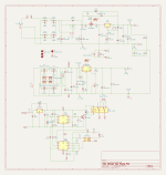
Schematic:

Rendered and Stuffed:

I will be updating the first post soon enough, but here is the v1.1 schematic, BOM, board layout, top and bottom tracks, and 3d renderings.
At this time I have not posted the gerbers themselves but will happily post them if people request it. I am happy to be the guinea pig for initial testing and will be placing an order shortly with JLCPCB for a set of 5 boards, 1.6mm thick with 2oz copper. When the board is tested and validated as good, I'll get to work on our LR8 based version. Though I am confident in the LM317 board, the one place I am not certain is the MIC29153/303/503 LDO models and the error flag pin. This is elaborated on further below, but let's talk about the board itself.
The Board:
Dimensions are 182mm long by 104mm wide. Given current potentials in the low voltage section it is strongly advised for 2oz copper weight.
High Voltage:
High voltage input accepts single/parallel secondaries, center tapped transformers, and even tube rectifiers. The BOM notates which parts to omit depending on your high voltage needs. Users can use this as a CLC with an off board choke via L1 and L2 terminals on J9, or a CRC by populating R13, this does require the user calculate R13 value and power rating per output voltage needs. This feeds an LM317 based high voltage regulator that is capable of a wide range of output voltages.
With R16 (marked USER) for the HV regulator, the following resistor values are listed with details on the HV DC output voltage range. This is based on R19 being 250 ohm giving an adjustment pin current of 5mA for the LM317 which has an internal Vref of 1.25VDC.
With trimpot RV3 having a value of 10K (single or multiturn) the pot dissipation will be a max of 0.25watts if the wiper is sitting at the HV GND point with 50VDC across the pot. Then R16 will give the following:
R20 = 22K 3W - output HVDC range will be 110 to 160V
R20 = 27K 3W - output HVDC range will be 135 to 185V
R20 = 33K 3W - output HVDC range will be 165 to 215V
R20 = 39K 3W - output HVDC range will be 195 to 245V
R20 = 47K 3W - output HVDC range will be 235 to 285V
With trimpot RV3 having a value of 15K (single or multiturn) the pot dissipation will be a max of 0.375watts if the wiper is sitting at the HV GND point with 75VDC across the pot. Then R16 will give the following:
R20 = 22K 3W - output HVDC range will be 110 to 185V
R20 = 27K 3W - output HVDC range will be 135 to 210V
R20 = 33K 3W - output HVDC range will be 165 to 240V
R20 = 39K 3W - output HVDC range will be 195 to 270V
R20 = 47K 3W - output HVDC range will be 235 to 310V
Our transistor selected is an STP11N65M2 zener protected MOSFET mounted at the edge of the board with a heatsink footprint, or if a user desires, a notch in the board for underside mounting and chassis heatsinking.
High Voltage Delay:
Sandwiched between the high voltage and low voltage sections is a NE556 timer based relay circuit to delay the high voltage input to help protect tubes. This circuit obtains power by tapping off the low voltage regulator circuit right after the first filter capacitors. Included in this is an LED (D7) that will blink once per second while the timer ticks down, and goes solid once the relay is enabled. By default this circuit is set to 30seconds, but can be increased or decreased by adjusting the values of R6 (2Meg default) and C14 (15uF default) accordingly, 3Meg would give you roughly 45 seconds. For this circuit I started by following along Pete Millett's muting delay board and re-tailored it for our needs here.
I use Pete's board in a few preamplifiers and am very pleased with the functionality and it seemed like a good fit here. Pete advises that C12, C14, and C17 must be low leakage tantalum capacitors and I do not consider myself knowledgeable at this time to know why. The currently chosen tantalum capacitors are inexpensive and should work just fine, however if people would prefer we swap this board over to electrolytic capacitors, the footprints will accommodate that currently, and I can formally change the board, schematic, footprints, and bom quickly, I already have some caps bookmarked just in case.
The relay chosen here is an Omron G2RL-2-DC5 DPDT, which has a common footprint with some TE and Panasonic relays. Rod Elliott recommends that the relay contacts be rated for 250VAC or greater, there is also a varistor connected across the relay contacts as an extra precaution.
Board Grounding:
At the corner of the board is a built in loop breaker circuit composed of a CL-60 NTC and a 0.022uF Y2 capacitor. The nearby mounting hole is connected to the adjacent solder pad marked "chassis". Simply connect a jumper between the two "chassis" solder pads to connect the board to your chassis, or use the top chassis solder pad to connect via wire. There is also a "Gnd" solder pad for access to the high voltage circuits ground.
Low Voltage:
The low voltage circuit is based around the MIC29152/302/502 and MIC29153/303/503 models of LDO. There are several models spanning a variety of current capabilities, sadly they all seem to be in short stock lately, which is why we set out to accommodate them all. Models ending in 2 require J2 pins 1 and 2 shorted as that model pin 1 is an enable pin. Models that end in 3 change pin 1 to an error flag, reading the datasheet I believe this could be used to light up an LED if the error flag is enabled. To utilize models ending in 3 a user must short J2 pins 2 and 3. Alternatively if the error flag does not function as I expect, one can still use the 3 models by not shorting anything on J2.
R11, R12, and C21 will provide an elevated ground to 1/4 of B+ output for the filament regulation circuit to keep hum to a minimum.
The low voltage circuit can output 1.24VDC to 13.96VDC at up to 4.5amps of current. Anything above 2 amps of current will require that D1, D2, D4, and D5 are all connected to heatsinks. To accept a wide variety of tubes J5 is in place as a simple voltage doubler, this way 12V filament based tubes can be utilized with little more than a jumper swap and trimpot adjustment. Shunt J5 pins 1 and 2 for a voltage double circuit, or shunt J5 pins 2 and 3 for normal operation.
A Note On Footprints:
We are in a parts shortage, there's also a wide variety of choices for trimpots, as such I thought that I might be able to create a footprint that can accommodate just about any trimpot someone can find within reason. I mentioned it earlier in the thread but will bring it up again here. When seeking out a proper part for the trimpots, I found a variety of footprint patterns and pin numbering arrangement, and I think I've come up with a simple but small footprint that should allow a user to pick from many different trimpots to suit their needs or current part availability. The footprint is a 3x3 grid of 2.54mm spaced pins. One row for pin 1, one row for pin 2, and one row for pin 3, hopefully clearly labeled. Here's an image of the footprint as well as some example footprints that would all work. See the images below.
Footprints for electrolytic capacitors support multiple pin pitches to allow for as much user choice as possible without cluttering the board with too many solder pads. The small resistor footprint is sized to fit just about anything in the 0.5W to 0.6W range, as you'll see in the BOM it's mostly intended for Vishay / Beyschlag MBB series in 0.6W rating. Larger 3W and 5W resistor footprints are compact but will fit a wide variety of models. 3W resistor footprints are intended for use are CPF, FMP, HHV, PR03, RR. Inputs and outputs are sized to fit 2 pin and 3 pin 5.08mm pitch terminal blocks, however solder pads are large enough to allow direct to board wiring. We've also included test points for both high and low voltage at regulated and unregulated points.
Gerbers:
As mentioned, I am tentatively holding off on posting gerbers until I have tested and validated the board functionality, however if people want to join in the testing party, I am happy to share them. Earlier in the thread it was indicated that while JLCPCB may not charge you for a fleet of vias, other board houses may, as such I have produced a set of gerbers with 1,386 0.2mm vias joining the top and bottom ground planes together, as well as a set of gerbers containing no ground plane vias.
BOM:
I've attached the BOM in .pdf and .xlsx formats. I've included links to mouser and digikey for parts, as well as some sub parts that I think will be valid for use here.
Schematic:
Rendered and Stuffed:
Attachments
The heatsink pads are unconnected, but it is always advised to use insulation. The BOM should have heatsink mounting kits listed.I’m assuming isolating tabs to heatsinks? The HS looks grounded.
The heatsink pads are unconnected, but it is always advised to use insulation. The BOM should have heatsink mounting kits listed.
The renders seem to show ground plane connection. I agree on grounded heatsinks for safety. Although for running a LT3080 a output HS also helps the datasheet in using a driven ring guard (ie HS in addition) - it was purely by accident as intended it to be isolated, it turned out 150Vdc. Luckily the other grounded heatsinks are a distance away.
I went ahead and updated the initial post in the main thread with the information from post #70. Added in statements that heatsinks must be insulated. Updated BOM with corrected heatsink numbers and added optional 14 pin DIP socket.
Just wanted to give everyone a quick update. I've built up a verification board, and tonight I got the time to fire it up on the "bench" (Costco kids table! 😀 ), I am feeding it from an AS-05T120 using the 100V high voltage winding and the 6.3vac windings, I populated R13 with a 5W 1K resistor, R16 is populated with a 22K 3W resistor, and RV3 is a 10K 3296W. Currently I have no load on it, and have been running it idle for over an hour with no issues, low voltage is dialed in at 6.30VDC and high voltage with the adjustment pot set to the lowest.
I am very pleased to say that all of the core functionality of the board is working as expected. The low voltage circuit is working and adjustable, holds stable. The high voltage delay circuit works albeit with a tiny flaw that I am working on figuring out now, if anyone has any thoughts or insight I am glad to hear it. More info below. Once the high voltage delay enables the relay, the high voltage section regulates voltage as expected, trimpot works to adjust high voltage although it's a bit slow to respond so be patient. I've never used a Maida style regulator before so I do not know if that's expected or not. Albeit a board with no load right now, checking temps with my IR temp gun shows a barely above room temp board.
There are a couple of flaws that I uncovered while building and initial startup, the board has either been updated or I am working on correcting it now.
Board tweaks implemented:
Connect a simple single 6DJ8 tube circuit and apply load. Assuming the single tube circuit is stable under load for a couple of hours, I will look into rigging up a higher voltage transformer and a board that has 2x 12AX7's and 2x 12AU7's to test under higher load.
I have a Hantek 2C42 handheld oscilloscope and a Hantek DSO2D15 oscilloscope. I'd like to measure the noise of the power supply, but not sure where to start, if anyone could point me towards some guides to read that would be fantastic.
Here's a picture of the board idle under no load!

I am very pleased to say that all of the core functionality of the board is working as expected. The low voltage circuit is working and adjustable, holds stable. The high voltage delay circuit works albeit with a tiny flaw that I am working on figuring out now, if anyone has any thoughts or insight I am glad to hear it. More info below. Once the high voltage delay enables the relay, the high voltage section regulates voltage as expected, trimpot works to adjust high voltage although it's a bit slow to respond so be patient. I've never used a Maida style regulator before so I do not know if that's expected or not. Albeit a board with no load right now, checking temps with my IR temp gun shows a barely above room temp board.
There are a couple of flaws that I uncovered while building and initial startup, the board has either been updated or I am working on correcting it now.
Board tweaks implemented:
- corrected instructions for jumper usage, jumper silkscreen labels were reversed
- moved high voltage input and choke/rect input labeling so it's not blocked by a terminal block
- changed BOM C21 part as footprint on board is smaller than one previously listed in BOM
- updated BOM preferred shunts to be 13.97mm tall open top with grip for easier use
- slightly increased TH1 pad holes from 1.0mm to 1.2mm, CL-60 has 1.0mm leads
- I stupidly sandwiched the low voltage unregulated test points between the 4 big 15K uF caps and they aren't really easy to get to, I'll get those moved up near R3 by the low voltage outputs
- LED blinks as expected it blinks during delay period then after relay enables the LED turns off for ~30 seconds and then goes solid
- working on correcting that now but not entirely sure where I went wrong
- The expected behavior is LED to blink during the delay period and when the relay enables go solid
Connect a simple single 6DJ8 tube circuit and apply load. Assuming the single tube circuit is stable under load for a couple of hours, I will look into rigging up a higher voltage transformer and a board that has 2x 12AX7's and 2x 12AU7's to test under higher load.
I have a Hantek 2C42 handheld oscilloscope and a Hantek DSO2D15 oscilloscope. I'd like to measure the noise of the power supply, but not sure where to start, if anyone could point me towards some guides to read that would be fantastic.
Here's a picture of the board idle under no load!
Last edited:

Thanks Vunce! So far so good, soaking up 9.7watts at the outlet, 120v US. The circuit below is what I have running on it right now, no audio connected just voltages, and a cheap chinese tube incase something goes wrong. Been running ~1.5hours now without any issues.

The WAGO's are a game changer, I think in another thread I saw you posted a picture with a mount for them, another game changer that will beat my epoxy to the chassis method.
The WAGO's are a game changer, I think in another thread I saw you posted a picture with a mount for them, another game changer that will beat my epoxy to the chassis method.
After a bit of a late night poking and prodding at the board, and cracking back at it when I woke up, I finally got the LED behaving as expected. I make no claim as to the resolution being my design, I was just doing some googling and found the answer.

That schematic says to add a 1N4001 diode between the output of the relay delay circuit, and the reset pin of the LED flasher circuit, and right after the diode a resistor to ground. I figured what the heck, I'll give it a shot. A little trace cutting, some rigging, and we are in business!

I've gone ahead and incorporated this into the PCB and BOM already and will update the first post shortly. I've also added a terminal block near the high voltage relay for an off board LED.
That schematic says to add a 1N4001 diode between the output of the relay delay circuit, and the reset pin of the LED flasher circuit, and right after the diode a resistor to ground. I figured what the heck, I'll give it a shot. A little trace cutting, some rigging, and we are in business!
I've gone ahead and incorporated this into the PCB and BOM already and will update the first post shortly. I've also added a terminal block near the high voltage relay for an off board LED.
I used a cap multiplier and voltage tripler to get 126v B+ from 145v tripler output.
Hum is below the 6922 triode noise.
Hum is below the 6922 triode noise.
- Home
- Amplifiers
- Power Supplies
- The Ultimate Tube Preamp Power Supply