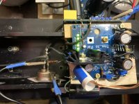
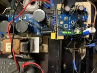
Well, it plays. Sounds a little diminished in level.
Certainly doesn't sound obviosly distorted
Certainly doesn't sound obviosly distorted
it is safe to work on it further
now - schematic as is , range of voltages with 5K trimpot (P2 on SIT board ) is from -1V7 to -4V17
put back everything as it was, I mean - R10, R11, R12, P2
do not touch trimpot at MOS board
then try everything again
maybe best solution is to clip drain wire of SIT (so no juice in mosfet and SIT, violet wire in post #2) , then confirm what you're getting with P2 in both opposite positions ....... and that will be confirmation of P2 functionality ( it hopefully isn't flashed in any of possible escapades)
when you are done with that, reconnect violet wire and try to set output node voltage to prescribed value
if you're short volt or few, increasing R11 slightly (without touching any other resistor) will do the job
say that you have 3K3 in place of R11 , that means range of -3V2 to -5V1
and, please - whatever you do, write clearly what is changed and give me all values from last schematic , those in red ( except 20mV across R9, you're not going to change it)
Ma bucur foarte mult pentru aprecierea ta, multumesc🙂Construcție excelentă
OK, I will refrain from pictures in the future 🙂🙂Beauty in simplicity ......... of overkill

But still it's an amplifier with a sound that I really like and I'm not sorry I did it that way
I don't speak English and I don't always understand the answers you give 😉
But from the translation I understood that "I exaggerated and the simplicity is the best"🙂
But from the translation I understood that "I exaggerated and the simplicity is the best"🙂
Mighty ZM using same translation service :
frumusețea este în simplitate ...............
..... simplitatea exagerării
yup, it's hard when using Translators ; so , you got nothing but nice words for your work
frumusețea este în simplitate ...............
..... simplitatea exagerării
yup, it's hard when using Translators ; so , you got nothing but nice words for your work
90V would demand changes in some resistor values, both in Mos part of circuit and SIT part of circuit
and quite bigger heatsink on IRF510
major benefit should be higher working voltage for SIT (better linearity, lesser THD) but .......... question is - do you need more power from SE SIT amp?
if you really prefer what you are getting from that sort of amp than from some other (higher power one), change damn speakers - to ones needing less power
point is - A Class amps are best suited with more efficient and more sensitive speakers - they're simply parts of same Fairy-tale
not that you can't use more HiFi speakers, but I'm sure that enjoyment level is - if ot greater with "Old School" speakers, then at least is easier to reach that level
example - Papa's PL SR1 are maybe best HiFi-approach made speakers I have heard (mucj more brain in them than visible outside, believe me) but his big honking Tanns are simply more fun
call me biased, that always I am
dunno how all this will go through translator to Romanian, but I tried my best 🙂
and quite bigger heatsink on IRF510
major benefit should be higher working voltage for SIT (better linearity, lesser THD) but .......... question is - do you need more power from SE SIT amp?
if you really prefer what you are getting from that sort of amp than from some other (higher power one), change damn speakers - to ones needing less power
point is - A Class amps are best suited with more efficient and more sensitive speakers - they're simply parts of same Fairy-tale
not that you can't use more HiFi speakers, but I'm sure that enjoyment level is - if ot greater with "Old School" speakers, then at least is easier to reach that level
example - Papa's PL SR1 are maybe best HiFi-approach made speakers I have heard (mucj more brain in them than visible outside, believe me) but his big honking Tanns are simply more fun
call me biased, that always I am

dunno how all this will go through translator to Romanian, but I tried my best 🙂
I listened to this amplifier for over an hour last night and it did not misbehave in any audible way.
I intended to connect up ROOM EQ WIZARD and see how it measures compared to its counterpart on the other channel and I will do that this evening. Curious how much level is missing and how the REW distortion plots compare. Just for fun.
You had mentioned how non-critical the SITs are and it sure seems to be even truer than you may have thought.
I do have my suspicions about P2, too.
I keep thinking that something more than the 510 was damaged by the solder blob bridge?
I will do as you ask this afternoon when I return home.
20mV across R9 is saying that JFets are well and alive
proper voltage at IRF gate and source are saying that IRF is operating as needed, serving as voltage umbrella for JFets
you have 12V going from LM317, so that's good
check resistors you did poke, same as trimpot (measure outer but also from outer to mid pins, to confirm wiper contact; desolder it for that)
and that's it - just follow literally what I wrote in last post and it'll be good; do not follow your creative impulses now, work with me ...... 🙂
Well, you do know me well.
I have learned over the decades that I learn much more from making mistakes than doing things correctly.
You have settled my mind with the above post - as if you were reading a plonker's brain ...
I will be as ZMesque methodical as my emotional Scots brain will allow. I( have told it to be on its best behavior.
I am still at work.
Will be leaving soon.
EDIT CORRECTION: This is not the amplifier I am having this trouble with - it is #1.
So just to answer a nagging question - where is all of that voltage that should be between drain and source hiding? Is the mosfet absorbing it all?
I am going to remove the "purple" wire and see what P2 does first. I will let you know as soon as I know the answer. Everything else had been put back to "OEM" yesterday.
THANKS, ZM
Last edited:
OK, I removed the "purple" wire.
I connectd ohmmeter across resistor R10 and it is obvious trimpot works.
Where do I measure the voltage for this:
maybe best solution is to clip drain wire of SIT (so no juice in mosfet and SIT, violet wire in post #2) , then confirm what you're getting with P2 in both opposite positions ....... and that will be confirmation of P2 functionality ( it hopefully isn't flashed in any of possible escapades)
Would this be between R11 and R12? That is what I assume and will give it a try.
disconnecting "violet wire" is writtena nd prescribed as part of procedure
I want confirmation of all voltages in red squares, from last posted schematic
all are referenced to GND, which means black probe to gnd, red probe to where red line from square is touching near circuit line
and yes, for biasing voltage - please for both trimpot extreme positions
so, please, go back and re-read procedure I wrote in post #662, and simply follow it
- Home
- Amplifiers
- Pass Labs
- The Singing Bush Tips 'n' Tricks

