After testing the first channels connections to the power supply using a dim bulb tester, I completed the above steps.- fire up that channel ; LEDs are lit!!, so most probably IRF is prepared to give some juice for input JFet buffer
-twiddle P1 to get 20mV reading on meter, which means buffer Iq is set to 20mA, which is enough juice even for controlof BigHonkinSIT
-just for fun, find trace where you can check what's voltage at IRF source ( that's positive rail for buffer) - there is plenty of possibly empty pads for T092 JFets ; expect aroundish 7V there
-just for fun, check what voltage you can set twiddling with P2 - you can use SIT Gate pad for red probe ; so , you confirmed that twiddling with P2 is giving a change, now set it to max neg voltage and be done
-power Off the entire Shebang, do the same procedure with other channel
LEDs are lit! Was able to adjust P1 to the 20 mV. I was able to adjust P2, the maximum I was able to achieve was -3.98 vdc. DC offset was around 25 mV.
However, my rail voltage is 71 vdc. I'm using 48v secondaries because I had it around. Before I connect the Drain wire to the SIT, is the rail voltage excessive?
more the merrier
take care of not exceeding caps voltage (output cap)
take care of temperature of IRF510; if needed - increase size of small heatsink
feel free to set output node voltage (+ side of output cap) even higher than in case of 60-65V rail
btw. you're loosing me with "DC offset was around 25 mV"; where?
take care of not exceeding caps voltage (output cap)
take care of temperature of IRF510; if needed - increase size of small heatsink
feel free to set output node voltage (+ side of output cap) even higher than in case of 60-65V rail
btw. you're loosing me with "DC offset was around 25 mV"; where?
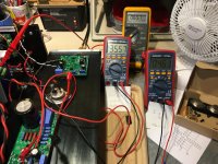
I had DVOM's across:
- Speaker terminals (DC offset?)
- Rail positive and negative
- R9 on SIT PCB
- Drain mount of SIT PCB to ground
The output cap is 63v, I'll get a bigger heatsink for the IRF510.
If I increase the output node voltage past the 32v you had it adjusted to, what change in performance will occur?
If output node is 1/2 of rail, then is 35v good?
If I increase the output node voltage past the 32v you had it adjusted to, what change in performance will occur?
If output node is 1/2 of rail, then is 35v good?
you can't have DC offset on speaker terminals, coupling cap is preventing that ..... so ignore whatever you did measure there .., simply phantom voltage
rest - 48Vsec will give aroundish 60Vdc, when loaded
rest - 48Vsec will give aroundish 60Vdc, when loaded
Am I ever glad I installed the 3-4A slo-blo fuse inline with the rail. I'm also glad I bought lots of fuses.
Just so I understand, the first adjustment (measured across R9 on the SIT PCB) is adjusted using P1 on the SIT PCB to 20mV.
Then I adjust P2 (red probe to SIT GATE pad) for maximum negative voltage.
Turn off everything and wait until rail measures 0V.
Connect big wire with eyelet to gate of SIT.
Voltmeter to SIT DRAIN (Output Node voltage), second voltmeter (Iq)across R5 or R7 or up to R13
Adjust P1 on MU PCB to 460mV
Adjust P2 on SIT PCB to 34 - 37 v.
Adjust other channel, same way!
Let it bake and adjust for 460mV and 34 - 37 v. with lids on.
Just want to make sure before I go kill some more fuses.
I had problems because of initial adjustment of P1 x2 and P2 for maximum resistance, I had to remove the MU PCB from the MOSFET to get P1 (on MU PCB) adjusted to Maximum.
it sounds proper as you wrote it....... almost!!!!!!!!!!
unconnected wire in first steps is wire going from Mu pcb to DRAIN of SIT
unconnected wire in first steps is wire going from Mu pcb to DRAIN of SIT
Yes, first part is for SIT PCB buffer Iq, second part is for SIT Iq and Output Node Voltage.
Every time I connected the drain wire to SIT, I would kill fuse and LEDs on SIT PCB would go out. Very frustrating until I decided to back to the beginning, and I found P1, P1 and P2 initial adjustment wrong.
Thank you again, now I feel comfortable with adjustments.
Every time I connected the drain wire to SIT, I would kill fuse and LEDs on SIT PCB would go out. Very frustrating until I decided to back to the beginning, and I found P1, P1 and P2 initial adjustment wrong.
Thank you again, now I feel comfortable with adjustments.

Here are some photos, I bought this enclosure last year because the heat sinks were 400mm X 150mm with an 8mm base. The inside of the enclosure is very narrow as you can see, the torroid was raised to allow the MU PCB to fit on the lower part of the heat sink. I'm using the Mark Johnson soft-start and dual power supplies using a single torroid. There are twin ground lift rectifier bridges with CL-60's in parallel between the filter caps (27K X 2 @ 80V) and the soft start board on the rear cover. The top and bottom covers are 5mm thick, the rear is 3mm and the front is 20mm.
Attachments
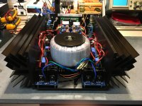
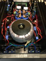
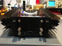
Very tight fit!
Suggestions that might help in noise control:
- separate the Ground input and output at the power supplies
- rotate the transformer to find the position of least noise. My experience with Antek transformers is that they leak at the wire output locations. Line them up with the front and back of the chassis for least noise.
The resistors in the CRC circuit will get hot. Keep wires away from them.
 .
.
Suggestions that might help in noise control:
- separate the Ground input and output at the power supplies
- rotate the transformer to find the position of least noise. My experience with Antek transformers is that they leak at the wire output locations. Line them up with the front and back of the chassis for least noise.
The resistors in the CRC circuit will get hot. Keep wires away from them.
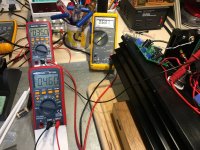
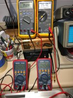
I let it bake for three hours last night, this morning I connected the DVOMs and let it bake for two hours, reset Iq and Output Node voltage. It then baked for an additional two hours, very stable.
I have some chores to do around the house, I hope to hear music from it tonight or tomorrow.
You will be the second to hear the results, my wife will probably hear the music before you.
I have some chores to do around the house, I hope to hear music from it tonight or tomorrow.
and?
You will be the second to hear the results, my wife will probably hear the music before you.
Attachments
She's The Boss

(as soon I did confess that, my life became easier .... now I can do whatever I want, I have permission)
(as soon I did confess that, my life became easier .... now I can do whatever I want, I have permission)
It plays BEAUTIFUL music! I'm off as far as the proper resistor for the meter to be at mid scale, very minor. I have a slight amount of hum, I'll try Ben Mah's suggestions this weekend and try to eliminate it. I have some 1 1/2" feet on order to raise it up for improved cooling.and?
For now I'm taking a victory lap! WOO HOO!
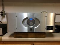
Here is the front panel, I know it's a kind of a copy of a famous amp designer, I wanted to build a "Tribute" amp. I've built a Jaguar XKSS replica and a Fast Five Daytona coupe, I've built engines for Cobra replicas/Tributes, but I've never owned one.
So here is my version of a Pass Tribute amp by Zen Mod.
Attachments
- Home
- Amplifiers
- Pass Labs
- The Singing Bush Tips 'n' Tricks