salas a quick sim in LTspice for the Bib resulted with decently flat op impedance but what about the phase angle isn't that affects the linearity?
at 100Hz its 118 degrees and at 10Khz its at 223 degrees. AFAIK i think phase angle also plays a significant role isnt it?
at 100Hz its 118 degrees and at 10Khz its at 223 degrees. AFAIK i think phase angle also plays a significant role isnt it?
Its not open loop phase. Zo phase I don't think its important. Especially the simulated one. See the sims in the BIB guide also. In any case no weird bumps though, smoothly progressive.
Hello Salas,
i want to build a 15v /350mA Salas shunt to replace my Young DAC power supply. Is the Reflektor D in post #2 the way to go, there are any pcb available somewhere ?
Do you have any specific building recommendation for this voltage an current ?
Thank you !
Adrian
i want to build a 15v /350mA Salas shunt to replace my Young DAC power supply. Is the Reflektor D in post #2 the way to go, there are any pcb available somewhere ?
Do you have any specific building recommendation for this voltage an current ?
Thank you !
Adrian
For 15V is either the "Reflektor general idea" link that you should build on veroboard (with higher V1, R6, lower R1) or the SSLV1.1 BIB that has some GB boards available periodically. It has specific pdf building and recommendations manual also.
Hi, does a specific build guide exist for the reflektor-d mini or is it all the same as for the regular reflektor-d build after the rectification and smoothing part of the circuit?
Thanks,
James
Thanks,
James
Hi James
It exists for the Mini refering to its build and there are special points for it to read but for the general stuff it links back to the original Ref-D's guide. I attach it here again for you to read it. Also see that post which explains the Vref elements pre-test process for the Mini to bits: http://www.diyaudio.com/forums/power-supplies/261031-reflektor-d-builds-71.html#post4710267
It exists for the Mini refering to its build and there are special points for it to read but for the general stuff it links back to the original Ref-D's guide. I attach it here again for you to read it. Also see that post which explains the Vref elements pre-test process for the Mini to bits: http://www.diyaudio.com/forums/power-supplies/261031-reflektor-d-builds-71.html#post4710267
Attachments
Stiff Salas with Negative Output Impedance (adjustable)
Greetings,
Not sure if this is the most appropriate thread for this (off-topic?).
If there is a better thread, please kindly advise.
I was recently pondering about creating a regulator with adjustable negative output impedance, so as to compensate for the voltage sag at increased current draw.
Initial fiddling (Spice, Soldered prototype) with basic LM317 and LM337 confirmed that the concept is defendable: An increase of output current resulting in an increase (or at least "no change" when optimized) of output voltage.
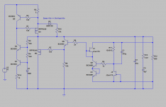
Encouraged by this, I came up with this version of a Duo-Salas Regulator.
Or maybe a Stiff Duo-Salas with adjustable Negative Output Impedance.
Does this make any sense to you guys?
A penny for your thoughts.
Cheers,
Ziggy.
Greetings,
Not sure if this is the most appropriate thread for this (off-topic?).
If there is a better thread, please kindly advise.
I was recently pondering about creating a regulator with adjustable negative output impedance, so as to compensate for the voltage sag at increased current draw.
Initial fiddling (Spice, Soldered prototype) with basic LM317 and LM337 confirmed that the concept is defendable: An increase of output current resulting in an increase (or at least "no change" when optimized) of output voltage.
Encouraged by this, I came up with this version of a Duo-Salas Regulator.
Or maybe a Stiff Duo-Salas with adjustable Negative Output Impedance.
Does this make any sense to you guys?
A penny for your thoughts.
Cheers,
Ziggy.
Attachments

Last edited:
... and this would be a slightly slimmer version, without the redundant overhead, but still with the adjustable negative impedance capability ...
Comments, anybody?
Is there some inherent flaw in this line of thinking
(apart the larger number of parts used)?
Comments, anybody?
Is there some inherent flaw in this line of thinking
(apart the larger number of parts used)?
Attachments
If it works in simulation you should test it in practice. In this there is a usually highly set current limiter and the voltage control element is in parallel though so not sure if solving much of a problem.
I think that will try to test this following variation. This time there are two sets of capacitors. But first, let's imagine an imaginary "mid-height reference" level, a "mid-ground" of sorts, cutting the schematic horizontally at half height. Any increased current draw spike originating from the load (R_load which is also cut in half by this "imaginary" mid-height reference) could result in:
1). a slightly falling spike of the positive voltage of the upper rail, and
2). a slightly increasing spike (a decrease of negative voltage => increase) of the lower rail, assuming that they are referenced to the imaginary "mid-height" reference.
This rising spike of the lower rail is conveyed by the lower set of (speed-up) capacitors to the base of the upper control transistor. This (imho) causes that this transistor closes up quicker and "harder" than as compared to / under normal conditions, as when its emitter sees only the falling voltage spike of the positive rail.
Vice versa,
The falling spike of the upper rail is conveyed by the upper set of (speed-up) capacitors to the base of the lower control transistor. This also (ihmo) causes that it closes up quicker and "harder" than as compared to / under normal conditions, as when its emitter only sees the rising voltage spike of the negative rail.
In essence, these sets of speed up capacitors should provide a measure of additional negative impedance "boost" under AC conditions.
In terms of DC conditions, The key player is and remains the central potentiometer (R106), the one that defines the output voltage level. Each of the current sources, both above as well as below this potentiometer, sees a slightly lesser value of the set resistance, due to the fact that there are two thieves. Current thieves. The R8 and R108 which are stealing part of the current from the sources, diverting it from R106 via an alternative path to the opposite rail.
Therefore, in the case of a long term variation of voltage at the output (say, voltage sag due to increased current draw by load), the amount of current that is being "stolen" by the thieves (R8, and R108) becomes lesser.
In essence, the current sources are hence "fooled" to believe that someone came and increased the resistance of the R106 potentiometer, effectively increasing the output voltage, i.e. compensating (or even overcompensating) for the hypothetical voltage sag that was experienced at the output in the first place.
Mind you, these are all just preliminary assumptions, that would need some verification in simulation and praxis. Question remains - if indeed, adjustable negative output impedance can be obtained in this way, does the anticipated functionality offset and outweigh the increased count of elements and complexity. Not to mention the other question, a question of stability.
Negative impedance sounds like an oscillations-accident awaiting to happen. For a person which is not equipped with a scope, it would be rather difficult to hand tweak the settings of the upper and lower pots, so as to achieve an optimum point. This would render the concept potentially useless for DIY'ers who are not equipped with a scope.
Comments kindly welcome. These are all early stage speculations, pertaining to a fresh concept, so maybe there is a flaw somewhere, but I do not see it yet.
Attachments
Last edited:
I am going to use this shunt reg to supply a Buffalo 3SE DAC wich demands 440mA,I´ll guess I set the shunt to about 500mA/5v
But now to the question should I use a 9 or 12v transformer?
I´m guessing a 12v?
But now to the question should I use a 9 or 12v transformer?
I´m guessing a 12v?
9V Tx should allow about 6.5V drop across the reg which is enough. 12V Tx should allow about 10.5V across the reg which is nice from less CCS Mosfet parasitic capacitance point of view but that Mosfet's dissipation will be 60% more i.e. 3.25W vs 5.25W. Its firstly a matter of sinking and ventilation capability in a specific build. Maybe 9V Tx and 540mA CCS is a good compromise.
Can please someone tell me on what pages I can find latest revision of the simplistic Salas shunt regulator schematic and pcb?
Thanks a lot!
Thanks a lot!
salas what will be the performance difference when we use shunt as BJT or MOSFET?
There are Zo sims in the bib manual to compare
Can please someone tell me on what pages I can find latest revision of the simplistic Salas shunt regulator schematic and pcb?
Thanks a lot!
See links from post#2 page #1
Hi Salas
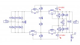
I am building a high quality power amp that needs 60VDC in the IPS and VAS and I believe the best way is to use a V12R to reg the rails.
I adapted your original schematic but am not sure I can use these trannies.... Will you please comment ?
I am building a high quality power amp that needs 60VDC in the IPS and VAS and I believe the best way is to use a V12R to reg the rails.
I adapted your original schematic but am not sure I can use these trannies.... Will you please comment ?
Attachments
Check the dissipations with holding Alt key when over the semis and doing left mouse click in LTSPICE .OP analysis mode. Better try to see what happens with TO-120s also like the BD series?
- Status
- Not open for further replies.
- Home
- Amplifiers
- Power Supplies
- The simplistic Salas low voltage shunt regulator