Hello guys,
I've seen that some of you have been using 2N5432 FETs in some of the reincarnations of Salas' design.
Does anybody have a source for these?
I'm building a Burst Generator board for my Audio Precision System One and need about 10 of these critters.
thanks,
jan didden
2N5457 in V1.2R is shown. 2N5432 is 0.15A min IDSS, can't remember designating such a (TO-18?) part myself. Its seldom and pricey on ebay too.
i'm perfectly satisfied with it 😉Nice shot, Thunderbirds grade.🙂 Did it all come across nice to ears too?
Another question: what is recommended capacitance in the filter before Salas Reg ? I thought to go with muscular 10.000 uF but I am not sure whether that is a good approach ...
10uF seems far too low for smoothing capacitance.
2200uF would be nearer the smoothing requirement.
2200uF would be nearer the smoothing requirement.
I will use 5kr for Vref // 10uF MKT on my p2p BiB clone, with three leds on the CCS.
Planning to use a 18VAC TX 50VA to get 14VDC out from the shunt.
Now I would apreciate your comments on the components connections so my build goes swiftly.
Does anyone detect any errors ?
Planning to use a 18VAC TX 50VA to get 14VDC out from the shunt.
Now I would apreciate your comments on the components connections so my build goes swiftly.
Does anyone detect any errors ?
Attachments
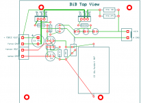
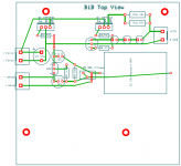
The sense circuit is a measuring bridge.
The -sense (GND) on you drawing feeds a bridge node on the S PIN of the jFET. Is that the correct place for the bridge node?
The +sense feeds a string of 4 components. Where is the bridge node?
BTW, I recommend changing the GND labels to - (or -ve, or NEG)
The -sense (GND) on you drawing feeds a bridge node on the S PIN of the jFET. Is that the correct place for the bridge node?
The +sense feeds a string of 4 components. Where is the bridge node?
BTW, I recommend changing the GND labels to - (or -ve, or NEG)
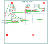
Thank you for your input Andrew.
Please forgive my lack of knowledge... What do you mean by bridge node ?
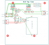
I compared this layout carefully with the BiB schematic and do not detect any errors... Would you please elaborate ?
Regards
Ricardo
Please forgive my lack of knowledge... What do you mean by bridge node ?
I compared this layout carefully with the BiB schematic and do not detect any errors... Would you please elaborate ?
Regards
Ricardo
Attachments
Last edited:
Are you familiar with a Wheatstone Bridge?
Look at an example. It is usually arranged as a diamond layout.
The top node and the bottom node are where the voltage is applied.
The side nodes are where the "error" is measured.
The the ratio of resistances on each of the two sides are compared. If the ratios are identical then the "error" voltage is also zero. A small change in the resistance of any one of the four legs/sides of that diamond will change the ratio on that side. Then you can measure the "error".
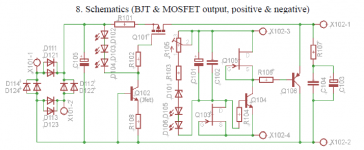
Using the schematic you have posted. I can see that for output X102-4 is connected to the bottom voltage. One could either choose the Source PIN of Q103, or the Emitter PIN of Q104, or the unlabeled junction between these two PINs. The Gate of Q103 must connect to it's Source PIN or to the measuring node. It must not connect to the other side of the voltage node, i.e. not to the Emitter PIN.
But when you come to look at X102-3 there seem to be 6 locations for the voltage node.
One must consider where the AC and DC currents flow and pick the node that best inserts the voltage so that the ratios are correctly measured.
Similarly when one comes to consider the side to side measuring Nodes, one must find the nodes that properly reflect where the error is correctly measured for both AC and DC outputs.
This is not a "pin the tail on the donkey" exercise.
This is precisely where the original DCB1 went wrong and some of the later incarnations were also wrong.
It took many posts, pointing out the mistaken layout, before the Members realised what they were doing wrong.
Look at an example. It is usually arranged as a diamond layout.
The top node and the bottom node are where the voltage is applied.
The side nodes are where the "error" is measured.
The the ratio of resistances on each of the two sides are compared. If the ratios are identical then the "error" voltage is also zero. A small change in the resistance of any one of the four legs/sides of that diamond will change the ratio on that side. Then you can measure the "error".
Using the schematic you have posted. I can see that for output X102-4 is connected to the bottom voltage. One could either choose the Source PIN of Q103, or the Emitter PIN of Q104, or the unlabeled junction between these two PINs. The Gate of Q103 must connect to it's Source PIN or to the measuring node. It must not connect to the other side of the voltage node, i.e. not to the Emitter PIN.
But when you come to look at X102-3 there seem to be 6 locations for the voltage node.
One must consider where the AC and DC currents flow and pick the node that best inserts the voltage so that the ratios are correctly measured.
Similarly when one comes to consider the side to side measuring Nodes, one must find the nodes that properly reflect where the error is correctly measured for both AC and DC outputs.
This is not a "pin the tail on the donkey" exercise.
This is precisely where the original DCB1 went wrong and some of the later incarnations were also wrong.
It took many posts, pointing out the mistaken layout, before the Members realised what they were doing wrong.
Last edited:
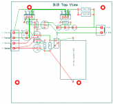
You don't need to bring both e & s to the -sense PIN.
You simply choose one, or the other, or connect the two PINs together and run from that trace to -Sense. That corner of the bridge is the easiest to get right.
I would connect the +sense to the top of VR3. This is an attempt to equalise the impedances of the traces to the drain PIN and to that physically far too big 10uF. That cap compromises the layout. But route that +sense trace alongside the -sense trace, i.e. under R3, under R4 and along past Q3.
The sense traces MUST have the absolute minimum loop area, it would be better if one trace was directly above the other, on either side of a very thin double sided PCB.
That brings up another reason for 10uF being too big. Any interference picked up by the loop area of the cap is read as an error signal ! Look at the loop area for the leads and the adjacent resistors.
Last edited:
10mF I guess he meant. 4700uF is a good mid value.
Sorry for late reply ... Yes I meant 10mF. 4700 uF looks good. Thanks Salas (and AndrewT) once again ...
Salas,
C3, should it be across the output terminals or should it be across the Drain and Source PINs of the Shunt FET?
C3, should it be across the output terminals or should it be across the Drain and Source PINs of the Shunt FET?
- Status
- Not open for further replies.
- Home
- Amplifiers
- Power Supplies
- The simplistic Salas low voltage shunt regulator