If it will run stable with the ''load'' as it is configured, leave it as it is. Test the rails with the actual circuit load attached and if its clean on the oscope then no need to tweak.
His Salas,
To makes sure that I understand, leave the caps installed, if it's stable on the scope, it's good to go, if unstable, then we will talk.🙂
Ken
Yes, see its stable as a reg alone on a dummy load resistor first. Like you got a DC line on scope, not some oscillation. If not so you play with some stopper values or you revise Mosfet choices/layout. If all is well, then you try with the actual load as it comes locally bypassed and all. Checking again. If something goes bad, we will see.
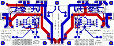
Since I recovered from my accident, I can finally put my PCB-layout to a test - I ordered all neccessary components and when they'll arrive, I will give it a try...
Actually some errors slipped into the design, when changing the layout on the negative side of the design by mirroring it - I forgot to change the markings of the components, but that should now be corrected...
Changes that were required:
- direction of 2N5457 swapped
- direction of 2SK170 swapped
- direction of BC556B swapped
- direction of BC560C swapped
Attachments
 Good luck, take care.
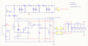
I think to use these schematics. The shunts elements are these transistors for audio applications: 2SC2690 (for negative voltage) and 2SA1220 (for positive).
I will make 8 regulators for my DAC. 3 - (+5V, -5V, -15V) for TDA1541A, 2 - (+5v, -5V) for clock, 1 - (+5V) for reclock, 2 - (+15V, -15V) for I/V stage.
I will be happy if Salas make his comment (for any errors or something didn't like). Excuse me for my English.
I will make 8 regulators for my DAC. 3 - (+5V, -5V, -15V) for TDA1541A, 2 - (+5v, -5V) for clock, 1 - (+5V) for reclock, 2 - (+15V, -15V) for I/V stage.
I will be happy if Salas make his comment (for any errors or something didn't like). Excuse me for my English.
Attachments

Last edited:
Output BJT only one guy from Ukraine had used for lower than 5V 1.2 up to now, and if I remember well he had problems and we made changes. Why not keeping with the output Mosfet, it can go down to 5V. Driving an inductive load is looking for oscillation. It also kills the very low Zout. You don't need extra filtering to the load. Also the red lines don't meet the black lines where the load is met in your schematic. They must meet at same points on the load.
Thanks for your answer. I wanted to use BJT, because they are very quietly. But if that isn't good - OK. Is that error if I use bypass caps? Murata DSS6N is EMIFIL element (ferrite beads with small cap). It has very small inductance. I understood for sense lines. Thanks.
Last edited:
Since you are specializing it, make a test build, try your BJT first, if problematic try your Mosfet, all in just a resistor load. If OK by then, try your real load. If problematic, simplify your load. Look on each step with oscope for no oscillation on the DC lines. Good luck, let us know. If you will look back enough there was a guy from UKR who put some in DAC. Maybe good to read.
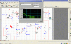
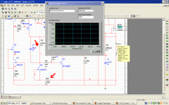
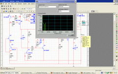
I don't like the output spectrum when C1=10uF. But that is only simulation. Look at the differences when C1=200uf. After I make a really test PCB I will do measurements with software TrueRTA and an external sound interface Emu Tracker Pre and will write for the results.
P.S. One interesting result. Instead LED ---> trimmer (as in the original Salas's schematic). The spectrum is clean.
P.S. One interesting result. Instead LED ---> trimmer (as in the original Salas's schematic). The spectrum is clean.
Attachments
Last edited:
Listen also with the film cap or the lytic cap there. I have been using both. You can also use 2SA970/2SC2240 if you got any instead of 560/550 & 546 for best noise.
P.S. One interesting result. Instead LED ---> trimmer (as in the original Salas's schematic). The spectrum is clean.
Neither the trimmer is sooo good nor the Led is sooo bad as in simulation. Best is (and audible) after you trim, substitute a low ppm metal film to the value you will find with the trimmer. Wait half an hour in actual final enclosure to determine that. There will be Tc slide in the Jfet, and contact play in the trimmer.
Thanks for help Salas. I will try and 220nf styroflex for bypass C1, too.
For R1 and R15 I can use very low noise Metal Oxide resistor Tesla TR-163, TR-161.
For R1 and R15 I can use very low noise Metal Oxide resistor Tesla TR-163, TR-161.
Last edited:
I also use MKP1837 or FT1 Teflon for bypass, its interesting to compare how they marry with the main film cap. R15 (trimmer) is located between Q4's source and ground by the way.
It's alive!
Salas,
Success! Tested the positive side with a 330ohm resistor load, 32v in about 22v out (didn't have time to set voltage) no oscillations, everything is good. Goofed up on the footprint of the Wima caps, but, fortunately had other film caps on hand at 4.7uf that I could mount on the bottom of the board.
Now onto a voltage doubler and cap multiplier.
Thanks for all your help.
Ken
Attachments
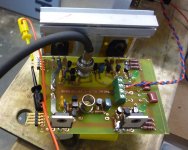
über looking board 🙂
Why the voltage multiplier ?
The shunt will power my LME49811 amp. I want to drive the 49811 at a higher voltage than the output stage.
- Status
- Not open for further replies.
- Home
- Amplifiers
- Power Supplies
- The simplistic Salas low voltage shunt regulator