I wonder if there isnt still a wiring problem. Tony have you measured the voltage coming into this board? I just want to make sure you have +/- 25 and 0V. I had a similar problem as I said with my etched boards when the relay wasnt clicking on. I had like 12.5V rather than 25. Redid everything only to find this was my problem.
Uriah
Uriah
Help Needed
Hi Uriah,
Yes, the toroids are rated at 24.5 but my MM reads 26Vac. The other board works fine with the same wiring.
Hi Uriah,
I just want to make sure you have +/- 25 and 0V.
Yes, the toroids are rated at 24.5 but my MM reads 26Vac. The other board works fine with the same wiring.
Help Needed
Cont.
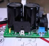
What I find very strange is that I had to put a wire between the two caps as shown on my pic. These should normally be joined together by that huge trace on the other side of the board. I may try to unsolder both caps tomorrow , swap them round and resolder without the wire and see what happens. Will first wait to see what Troy proposes.
Cont.
What I find very strange is that I had to put a wire between the two caps as shown on my pic. These should normally be joined together by that huge trace on the other side of the board. I may try to unsolder both caps tomorrow , swap them round and resolder without the wire and see what happens. Will first wait to see what Troy proposes.
I have a question in regards to my hum issue.
I experimented with running a jumper wire to ground on my right channel board and all the hum absolutely disappeared. If I permanently ground the pcbs is anything bad going to happen?
I experimented with running a jumper wire to ground on my right channel board and all the hum absolutely disappeared. If I permanently ground the pcbs is anything bad going to happen?
Just to be sure: do you mean that you connected power ground to the earth connector on the power?Coreyk78 said:If I permanently ground the pcbs is anything bad going to happen?
I do not have the training to give advice on proper grounding and power setup for safety. But I can tell you what I do. I do connect power ground to earth (and the latter to the chassis if it is metallic).
It has been pointed out by others on this forum that such a connection is possible and that some prefer to have an RC filter on that connection.
I found the writing of Rod Elliott on power supplies and how to hook them up useful on this subject.
peter
Yeah this is a topic that Peter and I will get a bit skiddish on. We dont want you hurting yourself somehow with our not so well informed advice.
So, with that disclaimer in mind and also considering the Brian and Russ both said to NOT ground to earth I will tell you that I am grounded with both amps to 0V but also to earth as well as all speaker and inputs ground. They all go to their respective place on the board but are then grounded to earth through two star grounds. WHY did I do that? Well I think if I had two of the kit boards that probably I would not be doing it this way, but I have a board without soldermask and maybe everything is normal on it but I dont think so. I have to ground this way or I get some serious DC to the speakers. Not the same problem you are having, but yeah some people are going to earth ground as well.
Uriah
Coreyk78 said:I experimented with running a jumper wire to ground on my right channel board and all the hum absolutely disappeared.
You know, its possible that we both have a bad solder joint somewhere in our power supply soldering to power ground and that maybe the amp is finding it easier to reference earth ground because of this.
Uriah
I printed the schematic.
I will be able to pull out my amp and test the points tomorrow for operating voltages.
Then I will post them as troubleshooting guides for future use.
I will also take a close up photograph of the PCB's to use as visual comparisons in the future.
But this will all take place in 12 hours.. Friday night here and my GF says it is her time... Till tomorrow I bid you adieu!
I'm talking about connecting power ground to earth. No magic smoke was released when I tried it, so I can probably get away with it, hehe.
some pictures
You may find some of the pictures I put up earlier useful for comparison http://picasaweb.google.com/schro20/FinalBuildOfRevCFromKit#
peter
You may find some of the pictures I put up earlier useful for comparison http://picasaweb.google.com/schro20/FinalBuildOfRevCFromKit#
peter
Hello,
Sorry if its sound funny, haven't solder in a while. Do we solder both the top and bottom pcb as well, or just bottom.
Ben
Sorry if its sound funny, haven't solder in a while. Do we solder both the top and bottom pcb as well, or just bottom.
Ben
I put flux on the holes (bottom of the PCB).
Place the components.
Hold with my finger
Flip the PCB component side down
Solder and ensure the solder fills the hole.
Then I flip the PCB component side up, reheat the joint and pull my soldering iron down the component lead to let gravity "pull out / wick away" excess solder.
Capillary action keeps the hole filled and the component securely soldered but the "extra" is taken out and the chance of a solder bridge on the top where you can't get to and see under some components is minimized.
My
Ok, the schematic is prolly useless in using for trouble shooting...
Where is a copy of the PDF's of the component side and the solder side of the PCB?
Does anyone have a copy? My originals from the Twisted Pair BG are on an old PC in storage..
I will print that and put voltage measurements on that...
What I am looking for is the top and bottom drawings to print out like what is under this PCB:
http://picasaweb.google.com/udailey/MyRef#5278313664886619282
Uriah-
Thank you.
That is one view that I needed, do you also have the bottom side?
And how do I print it larger than "actual size"? I am trying to manipulate it to be larger and fill up an 8 x 11 sheet of paper but it keeps printing as a 4 x 6 with LOTS of open area around it on an 8 x 11 sheet.
Thank you.
That is one view that I needed, do you also have the bottom side?
And how do I print it larger than "actual size"? I am trying to manipulate it to be larger and fill up an 8 x 11 sheet of paper but it keeps printing as a 4 x 6 with LOTS of open area around it on an 8 x 11 sheet.
Try 'print with preview' and center it then increase the percentage to like 150%.
Bottom side.... I dont know if I ever had bottom side. Let me poke around.
Uriah
Bottom side.... I dont know if I ever had bottom side. Let me poke around.
Uriah
udailey said:Try 'print with preview' and center it then increase the percentage to like 150%.
Bottom side.... I dont know if I ever had bottom side. Let me poke around.
Uriah
I actually copied and pasted the picture to MS Paint and then printed.. 😉
I know I saw the trace side before and I am 99% sure I have it on my PC in storage.. But not on my work laptop, and my personal laptop is on loan to a friend who's home PC got eaten up by the "downadup / conflicker" virus...
All rightie then...
So I think we should start off by ensuring the grounds are good and the proper voltages are in the right places.
1. You should have ZERO resistance from the tie points of the following pairs of caps and PGND.
a. C3 + 8
b. C6 + 11
c. C1 + 2
2. On the hot side of those caps you should have:
(for the C6 and C11 you can measure at the inside leads of R1 and R4 since they are raised and easy to get to.)
a. C3 = ~- 32.5
b. C8 = ~+32.5
c. C6 = +12
d. C11 = -12
e. C1 = ~-32.5
f. C2 = ~+32.5
g. C14 = +24
That will give use power to the sections.
- Home
- Amplifiers
- Chip Amps
- The new "My Ref" Rev C thread