also got it all single sided with 5 short wire jumpers
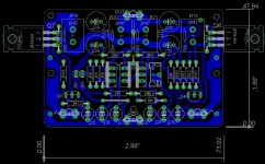
What's with J7, J8, J9 and R8? They don't fit where they are placed, across the FET's solder joints and underneath the resistors.
I think the board offers enough space to route them DIY proof, though. 😉
balanced input, what needs to be added to the original schematic to enable this option
I'm also (generally) very interested in this option.
Cheers,
Sebastian.
Last edited:
Hi sek, yes that jumper at the top right is a potential problem for kit builders, obviously I was only designing for myself at first. it is a very difficult spot to do anything else though, I will look at it again.
I will have to redo the BOM as my current one is for the SMD version.
The bulk of the cost goes into the heatsink, and transformer, which will set you back about $91 new at a pricey place like RS components, the rest of the parts can be dirt cheap or another $50 for fancy Welyn resistors etc... the psu caps will also be a few bucks.
Last edited:
Last edited:
Hi,
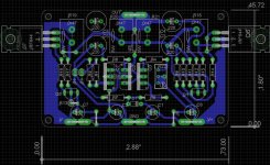
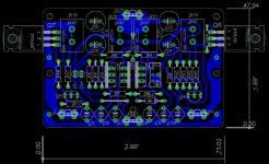
what's the actual case size of R18 through R20? Maybe they're actually smaller or elevated and allow for jumpers and resistors underneath? The MPC71 case (library 'resistor-power', device 'RMPC71-5') comes to mind (recommendable parts anyway, induction free 5W metal band resistors).
By moving J8 to the left of R7 or shortening it (so that the copper trace towards Q2 extends underneath R7) you could solve the overlap of R7 and J8.
By moving C2/J8 to the left and stretching J8, you could get rid of J5. Same goes for J6 by moving C1 and D1 to the right and rotating D1 by 90 degrees (thus D1 visualle 'mirroring' J8, probably only after flipping R5).
If you're brave enough to place R8 underneath the area of R20/R21, why not do the same with R14 and R18 in order to eleminate J7?
What's with R3 underneath Q1/Q2? Move R16/R17, the input connector and R2/R1 to the left by one resistor width and then place R3 adjacent to R4.
R13 standing upright? You'll be going to hate the looks of it with all the others laying flat. Why not move it next to R17 and pull the input connector downwards, next to Q5 (rotating R1/R2/R3 accordingly)?
Eliminating J9? Maybe with R17 to the right of R19 (level with R8 and possibly R14)? Might even enable you to leave the input connector where it is... 😉
Eliminating J8, finally? Only so much: Small capacitors (like C1, C2, C6, C7) usually come in both 2,5mm (1/10") and 5mm (2/10") pitch (i.e. device 'CPOL-USE5-5'). 😀
I'd also recommend giving the connectors a little more distance to the board edges (or flipping them 90 degrees, thus relieving the stress of cable force from the PCB edge and also allowing for angled connectors). At the very least consider using the device 'ST6,3' from library 'con-rib' (better force distribution).
And what's C8 doing up there? Teaming up with C4 for the looks of symmetry? 🙄
Just saying,
Sebastian. 😉
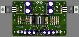
I designed around a vertical ceramic package with 5mm pitch, RS sells one in 5W, allthough only 3W is enough. I think useing a 5W unit will reduce surface temp, which is probably good due to proximity of electrolytics, but you should be able to fit a host of other resistors there.
R7 and J8 ; applied
By moving C2/J8 to the left and stretching ; I don't like it visualy, a great deal of effort went into getting things symetrical. J5 could be removed by simply routing the ground trace from C7, north of C2. This would however spoil the symetry with J6 to ground. To loose J6 also I would need to extend the path to ground for C6 by almost double. I have no concerns overt the jumpers in that position, I have seen whole sansui integrateds without a single ground trace on the PCB, all grounds were wires.
...do the same with R14 and R18 in order to eleminate J7; I actualy had thoughts around doing exactly that... might still. 🙂 the closer I get resistors to fets, the happier I am.
What's with R3 underneath Q1/Q2? ; nearly non existant signal lenght vs about a inch of trace, I think this one stays unless I get very good motivation to change it 😀
R13 standing upright ; breaks my heart, but doesn't look too bad in rendering, I realy miss the surface mount resistor in that position for shortest trace lenght. Maybe I should see what it looks like if I just throw it horisontal right there in position?
J9; could be eliminated by routing around path between R16 and R17, with 16 shifting a bit left.
Eliminating J8,; what about path to V-? I don't see how we'd loose the jumper regardless of cap size, I chose the 2.5mm pitch as it represents the largest group in that diameter.
Connectors were positioned to correspond with the wireing harness I planned to connect to the PSUs, the cables running in the corner along the bottom, I think I put up some renderings a few pages back... I'll swap to your 6,3 its just the pads that are diffirent?
C8 is there looking pretty 🙂
Are the 1/4" spade pads double sided?
Single sided are not as strong and with careless handling may fail later in life.
Single sided are not as strong and with careless handling may fail later in life.
I don't like it visualy, a great deal of effort went into getting things symetrical.By moving C2/J8 to the left and stretching
Symmetry is not a matter of looks, it's a matter of impedances and wave lengths. Besides, symmetry doesn't enforce leaving everything untouched, symmetry means moving the respective components accordingly. 😉
I have no concerns overt the jumper
Me too. It's just that this circuit doesn't need any when laid out on this board size. With the jumpers employed you could go much, much smaller, though.
Seriously and without any offense, I consider your argument of kepping things symmetric while randomly placing jumpers flawed in that you could either considerably ease the board by skimping on symmetric trace layout within justifiable means (whilst keeping parts neatly aligned) or improve looks and trace symmetry a lot by consequently introducing more jumpers.
However, RF aspects of trace lenghts and layout details are a whole new realm and will not be accepted as an excuse for arbitrarily shortening traces on this board. 😀
Ultimately, the number of jumpers can be choosen at will and as such is a matter of taste only. But no pressing here, it's your project and yours only! 😉
nearly non existant signal lenght vs about a inch of trace, I think this one stays unless I get very good motivation to change it 😀What's with R3 underneath Q1/Q2?
Motivation? How about everyone's ability to mount it - in contrast to 50% of potential builders failing (not to mention long term durability).
R3 does not closely couple Q1 and Q2, it rather sets the low side drive voltage (and thus doesn't directly affect the function of Q2). In other words, you could stretch this connection of V- to any length (within reason) without compromising performance.
Whichever way you pull out R3, at least flip Q1 then. Improves looks and saves you the hassle of routing that thin trace between the pads... 😛
Yeah, I figure. 🙄I realy miss the surface mount
You're doing a through-hole layout here, you can't have the benefits of both technologies while using only one of them. The implication: leverage on the benefit of easier mounting and forget the possibility of SMD-like compactness.
what about path to V-? I don't see how we'd loose the jumper regardless of cap size, I chose the 2.5mm pitch as it represents the largest group in that diameter.Eliminating J8
My recommendations weren't necessarily depending on each other. Eliminating J8 will be difficult when eliminating J5 at the same time. But think about it again with R3 near R1 and the input connector near R7. You're routing in between two pads of Q2. If you allow for that underneath Q1 your possibilites become endless... 😛
Speaking of which, with J8 moved down, why keep J5?!? Just remove it and adjust J6 accordingly.
I'll swap to your 6,3 its just the pads that are diffirent?
Yep, it probably just went into that library because it didn't fit into any manufacturer specific libraries, besides it being a standard part.
C8 is there looking pretty 🙂
😀
Cheers,
Sebastian.
Last edited:
Ssssssh Andrew, 🙂 Don't be so rough on your electronics man. Tell you what I do hate, are those RCA PCB connectors that go straight into PCB, not at 90 degrees.... especialy on something that gets plugged and unplugged as much as RCA cables. If properly soldered and a reasonable guage wire and connector is used on the spade, and not regularly plugged in and out, I see no reason it could not last indefinately... but from an engineering point of view, yes, top and bottom would have been stronger, but very wastefull if this is the only reason to add a second layer.
Also there has been some PMed requests to keep it as easy as possible to construct, and we all know how hard it is getting componets OUT of through holes, soldered on both sides, especialy when you are new, I remember stripping a piece of track on my brand new My Ref C boards, way back, like that.
I followed what I interpreted to be your instructions, but I am stuck haveing to use another jumber now to get power from V- rail..... (pic attached). Something else about the configuration of that point is, that I think idealy the V- side of R3 and Q2, should not be shareing a trace in the first place, and should idealy be seperatly decoupled (meaning i need to cram another cap in there if possible). I KNOW it will work just stitching stuff together, but I think with a little patience we can wittle down the compromises to a best case scenario.
The only thing I guess that is a bit of a negative, is that this layout would be a little harder on the DIY PDB fabricators, as a few pads are pretty close to traces and would realy benefit from soldermasks, which is a step few DIYers go to.
Attachments
Last edited:
Ok, brother, I managed to pull it off, just to satisfy my curiosity...
In the meantime my wife arrived home with the press and peel printout of the first layout I posted this morning. Comparing it with the final design, I have to say emphaticaly that I think it was better before... or maybe during some of the intermediary stages depending on taste.
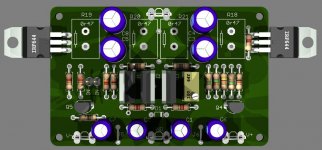
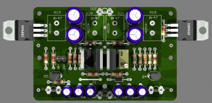
Where do I begin to explain.... firstly the board is tiny, not small, tiny. In fact you could fit two cahnnels on the palm of your hand. The reason for the small size is for optimal positioning on the heatsink, while leaving space for the rather large PSU section.
Previously traces were well seperated and spaced and appart from one spot running between the TO220's legs, soldering would be easy enough, provided you don't use one of those $3 100W irons from the dollar store. With the latter layout, we end up with a board literaly filled with traces, including some nasty combos. like power rail sandwitched between input signal before and after it goes through the first series resistor. Something in between the lines just make me instinctively say no when I look at it compared to the simplicity of the earlier routings.
Ultimately it wasn't a waste of time, as it allowed me to explore some routes I thought possible, but I am going to roll back a little, trying to keep the changes I thought were improvements and rolling back to some things I prefered/or accepted as compromises to achieve other priorities.
Also I want to find a way to decouple R3 and Q2 seperately if at all possible....
In the meantime my wife arrived home with the press and peel printout of the first layout I posted this morning. Comparing it with the final design, I have to say emphaticaly that I think it was better before... or maybe during some of the intermediary stages depending on taste.
Where do I begin to explain.... firstly the board is tiny, not small, tiny. In fact you could fit two cahnnels on the palm of your hand. The reason for the small size is for optimal positioning on the heatsink, while leaving space for the rather large PSU section.
Previously traces were well seperated and spaced and appart from one spot running between the TO220's legs, soldering would be easy enough, provided you don't use one of those $3 100W irons from the dollar store. With the latter layout, we end up with a board literaly filled with traces, including some nasty combos. like power rail sandwitched between input signal before and after it goes through the first series resistor. Something in between the lines just make me instinctively say no when I look at it compared to the simplicity of the earlier routings.
Ultimately it wasn't a waste of time, as it allowed me to explore some routes I thought possible, but I am going to roll back a little, trying to keep the changes I thought were improvements and rolling back to some things I prefered/or accepted as compromises to achieve other priorities.
Also I want to find a way to decouple R3 and Q2 seperately if at all possible....
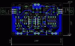
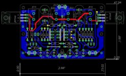
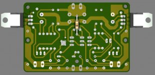
Did some quick markings in your picture.
The output current path is probably a little thin in trace width. Some other traces seem to somehow vary in thickness all over the place, too.
For DIY boards I recommend 1/25 in (~1mm) for low current signals and 1/10 in (~2.5mm) for higher current paths (i.e. power supply and output, marked red).
The copper rings of some component drills seem way thin (marked yellow). For the resistors I don't know how this happened, for the pot it's a property of the library design. As an easy fix, just place an artificial via of appropriate size on top of the holes (might even allow you to go for nicely round holes 😛).
The position of R17 doens't seem to allow for an increase output path thickness. Maybe now is the time to rethink your actual power resistor size requirements. And seeing that Q7 is sitting a little more inward than Q6, you might be able to finally make some room for R17, R8 and R14 up there.
Attachments
Last edited:
I just woke up from a nap, goddamn, I missed the postman, but I see the slip for my first signal generator is here!!!!!!!
Anyhow, yep on the pads, I was allready fattening them up like you said, I have to fix the libraries though, the FAB house gets a **** when you send tthem a drillfile with two drills on one hole coordinate.... I was just trying to share progress, those kind of things always gets a double lookover on the gerber files.
Agree on the trace thickness varying more than needed. I was thinking of pouring the red trace, but have doubts about turning it into an antennae. You'd have to forgive me, but I never got into the habbit of very wide tracks, probably because I'm poor and every mm of PCB I save generaly, counts. At the moment my traces are basicaly .8mm and 1.27mm for the thicker ones, appart from power rails.
Can you recheck your numbering for the last paragraph, you lost me there.... I'll see what I can do about the rest when I get your reply on that last bit.
P.S. do you rhink I am makeing progress or makeing it worse? 😀
Last edited:
Can you recheck your numbering for the last paragraph, you lost me there.... I'll see what I can do about the rest when I get your reply on that last bit.
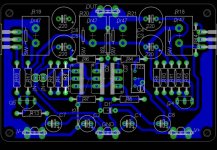
R17 is the resistor (connected to Q5) under which the power output trace bends through. Moving this one up next to R19 (similar to R14 near R18) would ease up things with the output trace and it's thickness.
Q7 slightly touches the left board edge while Q6 doesn't touch the right edge, thus Q7 could possibly be moved outward a little. Also, the resistor cases you incorporate might be way larger than required.
Accounting for these two aspects might make more room for the resistors R17 and R14 as well as the feedback resistor R8 (allowing it to be on the upper board side together with all it's friends).
P.S. do you rhink I am makeing progress or makeing it worse? 😀
I think you should stop worrying and start prototyping. 😀
OK, I'll jump on to getting busy again... Bad news though, RS components are backordered till 24 August for the output fets 🙁, I placed the order so long, but is there something cheap and nasty I could use to test functionality? I have some IRF540 and 640 I think.
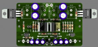
hey, like this?
Jep, like this. Although you might flip R13 up now. Y'know, for looks. 😛
Power resistors are correctly sized to within 2 digits past the decimal.
Just continue ignoring me on the industry standard for this type of application: MPC ... 😀
Cheers,
Sebastian.
Last edited:
- Home
- Amplifiers
- Pass Labs
- The Mini-A