Apex jr has some nice robust feet I haves used on several of my amps. They are on sale 4 for $2.00. can't beat that.Whats New at ApexJr
Attachments
Member
Joined 2002
Nice looking case, but shipping would be brutal!
Well, I received Brian's beautiful boards and and am starting to gather parts. DIY-Tech had most of the transitors and the rest I have coming from, hopefully, a good seller in Taiwan.
Being a little impatient to listen to an Aleph with my AKG K1000 headphones I also bought an already built Aleph Mini J from a seller on Audiogon. To my amazement it came with a set of Brian's amp boards already in it. The only difference that I can see is that the original builder used some 2sj74's instead of IRF9610's for the input transistors. The amp does sound very good however one channel has almost 100mv of DC offset on the outputs.
I have two questions. First. When I contacted the original builder he said that my best bet would be to replace Q1,2 with a better matched pair in order to lower the offset. I could do that but am wondering if there is an easier way to trim the existing circuit. Having said that I realize that it could be a problem since he did not follow Brian's parts list exactly and I have no schematic of his changes.
Second question: Do you think that making the amp into an "intergated" using a pair of 25K log pots would work? I suppose that it is no different than running the amp with a passive pre "driving" it but I was wondering if there would be any gotchas?
Thanks for any help and for the the input offered already.
Best,
Paul
Well, I received ............
study this :
Attachments
study this :
Thanks that is a big help. It goes into a lot more detail than some others I have been reading.
I know that it is better to remain silent and have others wonder if you are dim than to open your mouth and remove all doubt but here is another question 🙂
OK. Tonight I had the amp open looking at what it will take to replace Q1/2. While going over the boards I noticed something very odd. R13 had a broken or cut lead. The resistor had been mounted way above the board and as far as I could see had one side disconnected(cut) even though both leads were soldered. I figured that either it had snapped from some fluke. While getting ready to solder the two disjointed ends I noticed that the other R13 on the other board was similarly "cut".
Is this just a remarkable coincidence or did the creator snip it to take it out of the circuit on purpose? I do notice that the amp runs a little cooler with the resistors now back in the circuit.
Any ideas?
Best,
Paul
Member
Joined 2002
Thanks that is a big help. It goes into a lot more detail than some others I have been reading.
I know that it is better to remain silent and have others wonder if you are dim than to open your mouth and remove all doubt but here is another question 🙂
OK. Tonight I had the amp open looking at what it will take to replace Q1/2. While going over the boards I noticed something very odd. R13 had a broken or cut lead. The resistor had been mounted way above the board and as far as I could see had one side disconnected(cut) even though both leads were soldered. I figured that either it had snapped from some fluke. While getting ready to solder the two disjointed ends I noticed that the other R13 on the other board was similarly "cut".
Is this just a remarkable coincidence or did the creator snip it to take it out of the circuit on purpose? I do notice that the amp runs a little cooler with the resistors now back in the circuit.
Any ideas?
Best,
Paul
Pictures ? Did you buy this amp from some one ? It sure sounds like it!
......
Any ideas?
Best,
Paul
it will help if you post exact schematic from which is part nomenclature ;
this way I can't follow which part of schematic you're talking about
Pictures ? Did you buy this amp from some one ? It sure sounds like it!
Yes. I bought it on A-gon to use while building out Brian's boards. ironically, as it turns out is uses Brian's "black" boards!
It seems to use good quality parts although the builder did substitute 2sj74's for Q1/2 and seems to have left out a few other parts on the input. It sounds good although I need to work with it a bit to get the DC offset down on one channel ~90mv.
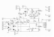
Here is Brian's schematic although my guess is that you are familiar with it. Sorry to not have included it...
On Brian's BOM it is listed as being 47.5K.
Attachments
Last edited:
R13 is snipped to ensure max possible bias of output mosfets , dictated solely by value of source resistors ;
without looking at your previous posts ..... give us few measurements data :
voltage across R28 or R27 , and value of these resistors ,
PSU voltages ,
value of R8,Z5,R18 ....... to check is it conversion to Mini Aleph J made without risks to input jfets
then I'll tell you how to set output offset without hassle of replacing input jfets
R13 is snipped to ensure max possible bias of output mosfets , dictated solely by value of source resistors ;
without looking at your previous posts ..... give us few measurements data :
voltage across R28 or R27 , and value of these resistors ,
PSU voltages ,
value of R8,Z5,R18 ....... to check is it conversion to Mini Aleph J made without risks to input jfets
then I'll tell you how to set output offset without hassle of replacing input jfets
Great. Thanks.
I was told that it is an Mini Aleph J (clone). I will check the voltages and parts values tomorrow when I am a little less sleepy!
Best,
Paul
Great. Thanks.
I was told that it is an Mini Aleph J (clone). I will check the voltages and parts values tomorrow when I am a little less sleepy!
Best,
Paul
Here is a bit of info from both channels:
R28 = .9/1.0 (in place)
R27 = .8/.9 (in place)
Supply is = +/- 17.64
R8 = .786/.769 (in place)
R18 = .995/1.012 (in place)
Zener - can't read the marking. Would I just measure the voltage drop across it?
Later....
Here is a bit of info from both channels:
R28 = .9/1.0 (in place)
R27 = .8/.9 (in place)
Supply is = +/- 17.64
R8 = .786/.769 (in place)
R18 = .995/1.012 (in place)
Zener - can't read the marking. Would I just measure the voltage drop across it?
Later....
please - write voltages across resistors ( yup - voltage across zener is fine ,instead of reading marking) and resistor values (read them, not measure in circuit)
few things from quoted post aren't exactly clear to me .
please - write voltages across resistors ( yup - voltage across zener is fine ,instead of reading marking) and resistor values (read them, not measure in circuit)
few things from quoted post aren't exactly clear to me .
Ok. With a steadier hand I ventured into the power amp and took some more readings. Here again I may share more ignorance than offer information...
The voltage across Z5 is 9.84v.
R28 measures .391v with one probe on ground and the other at the junction with R20. I read the color bands to be R=0.46 10%
R27 measures -17.55. I read the color bands to be R=0.46 10%
Thanks for working with me...
Best,
Paul
Ok. With a steadier hand I ventured into the power amp and took some more readings. Here again I may share more ignorance than offer information...
The voltage across Z5 is 9.84v.
R28 measures .391v with one probe on ground and the other at the junction with R20. I read the color bands to be R=0.46 10%
R27 measures -17.55. I read the color bands to be R=0.46 10%
Ok. I am going to take a stab at answering my own questions.
Regarding bias and R13. I got a reply from the builder and he snipped R13 to max out the bias at about 1.5 amps. Based upon his reply when I reconnected the 47K resistor I basically cut the bias in half. It definitely changed the sound but not for the better. With the resistor disconnected and the bias about 1.5a I could put my hand on the heatsink for about 15 seconds. 1.5 amps is probably max but workable so I will probably leave it disconnected.
Here is what his answer was:
"R13 is the dc bias resistor. snipped to full open let run at 1.5amp or so of bias rather than 1.1-1.2 amp if had 100k in there... tricky as orig aleph circuit has that resistor hooked up tiny bit differently, same purpose though (dc bias). Typically a 100k gives little over 1 amp, 150k 1.3 amp or so... 47k .8 amp."
My second question was the 90mv of dc offset. Reading Brian's schematic and comparing it to the Pass Aleph 30 schematic that I was pointed to it looks like R6 is used to adjust offset. The Pass schematic suggests 10M to drop the offset from ~100mv to a small number. Since the original builder of my board did not populate R6 this seems like the easiest solution as I could probably add it without pulling the board.
Am I on the right track?
replace R8 with 100R resistor in series with 100R multiturn pot
tweedle with pot , and you'll make offset vanish 😉
but - you didn't answered on all of my questions , so I can't tell you comment on what I'm also interested - what's current through input LTP
if values are as in original MiniA , then is possible that input Jfets are nearly overcooked .... but (skipping now to your previous post ) - looking at voltage across R8 (0V77? ) , if R8 is 220R , then input stage is starved ....
is it possible that you make new schematic , with exact part values , as they are on pcb ?
use this jpg ; it's probably more convenient than editing pdf ;
paste it in Paint , or whatever graf. proggie you are used
Attachments
replace R8 with 100R resistor in series with 100R multiturn pot
tweedle with pot , and you'll make offset vanish 😉
but - you didn't answered on all of my questions , so I can't tell you comment on what I'm also interested - what's current through input LTP
if values are as in original MiniA , then is possible that input Jfets are nearly overcooked .... but (skipping now to your previous post ) - looking at voltage across R8 (0V77? ) , if R8 is 220R , then input stage is starved ....
is it possible that you make new schematic , with exact part values , as they are on pcb ?
use this jpg ; it's probably more convenient than editing pdf ;
paste it in Paint , or whatever graf. proggie you are used
Ok. I see a problem. The values I posted were resistances, not voltages and I did not note that. And just to be really confusing I put in the values for both channels. I will edit them.
R28 = .9k ohms/1.0k ohm (in place, across the resistor)
R27 = .8K ohms/.9Kohms (in place)
Supply is = +/- 17.64 volts
R8 = .786K ohms/.769k ohms (in place)
R18 = .995k ohms/1.012k ohms (in place)
Measuring the voltage across R8 I get -8.23. The color code on R8 looks to my eyes like Br/Bl/Bl/Br/Br. Is that 1K 1%? ...which would be different from Brian's.
It may take a while to figure out all of the other resistor values given my obvious skills.
If it seems as if I am stuggling a bit through some learning here it is true!
hold your horses ! 😉
R28 and R27 must be in sub-ohm range .....
ok ; we are going to do it this way :
gimme :
R8 resistance and voltage across
R18 resistance and voltage across
R27 resistance and voltage across
R28 resistance and voltage across
Z5 voltage across
all resistance READ from part , do not measure in circuit
measure voltage ACROSS the part , not ref to gnd
I don't care for other parts - don't bother your self with schematic
and - give me values just for one channel - presuming that parts are the same on both channels , and that voltages are in 5% .
hold your horses ! 😉
R28 and R27 must be in sub-ohm range .....
ok ; we are going to do it this way :
gimme :
R8 resistance and voltage across
R18 resistance and voltage across
R27 resistance and voltage across
R28 resistance and voltage across
Z5 voltage across
all resistance READ from part , do not measure in circuit
measure voltage ACROSS the part , not ref to gnd
I don't care for other parts - don't bother your self with schematic
and - give me values just for one channel - presuming that parts are the same on both channels , and that voltages are in 5% .
Ok. No smoke, no shocks. I got the voltages across each device and read the resistors as best that I could. On for about 10 minutes. One channel only...
R27 = .47ohms with -.628v across it.
R28 = .47ohms with +.628v across it.
R18 = 1Kohms with -2.54v across it. (sort of drifted a bit)
R8 = 1Kohms with -8.69v across it.
Z5 has -4.59v across it.
R18 and R8 looked the same to me as far as the color code. br/bl/bl/br/br
Thanks for your patience!
OK
as I said before - replace R8 with 680R+500R trimpot in series ;
then adjust DC offset with that trimpot
which output mosfets you have in amp ?
2V54 looks somehow low for IRFP needs ....
as I said before - replace R8 with 680R+500R trimpot in series ;
then adjust DC offset with that trimpot
which output mosfets you have in amp ?
2V54 looks somehow low for IRFP needs ....
I built my mini-A using BrianGT's BOM. What is its input (unbalanced) impedance? Am I correct into thinking it's ~50K?
Last edited:
- Home
- Amplifiers
- Pass Labs
- The Mini-A