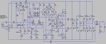
As alluded to early in the K10A thread, here are some teaser peeks of the big brother of my K10A hybrid amp (http://users.picknowl.com.au/~glenk/K10A.HTM).
This design uses On Semi RET devices for the output stage and, as in the K10A, a 12AX7 twin triode for the LTP. Split supply rails are used this time and the load is directly coupled.
Although not shown on the LTspice-drawn schematic attached below, the design incorporates a DC servo to null the offset voltage and has complete DC protection with a power up timer which allows the tube to warm up and the DC operating point to stabilise before closing the speaker relay.
The amplifier is rated at 25W into 8 ohms in class A and 50W into 4 ohms in class AB.
Quiescent current of the output stage is set at 1.3A and idle dissipation is approximately 65W.
Conservatively frequency compensated for a unity loop gain frequency of 1MHz, the simulated linearity is as follows:
25W into 8 ohms
THD-20kHz
0.001928%
THD-1kHz
0.000325%
1W into 8 ohms
THD-20kHz
0.000208%
THD-1kHz
0.000325%
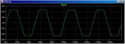
Full power bandwidth is in excess of 200kHz and particular attention was payed to clipping performance.
Within the next 6 months I hope to have a complete prototype built and boards for this design for sale.
Just starting this thread to gauge interest.
Cheers,
Glen
This design uses On Semi RET devices for the output stage and, as in the K10A, a 12AX7 twin triode for the LTP. Split supply rails are used this time and the load is directly coupled.
Although not shown on the LTspice-drawn schematic attached below, the design incorporates a DC servo to null the offset voltage and has complete DC protection with a power up timer which allows the tube to warm up and the DC operating point to stabilise before closing the speaker relay.
The amplifier is rated at 25W into 8 ohms in class A and 50W into 4 ohms in class AB.
Quiescent current of the output stage is set at 1.3A and idle dissipation is approximately 65W.
Conservatively frequency compensated for a unity loop gain frequency of 1MHz, the simulated linearity is as follows:
25W into 8 ohms
THD-20kHz
0.001928%
THD-1kHz
0.000325%
1W into 8 ohms
THD-20kHz
0.000208%
THD-1kHz
0.000325%
Full power bandwidth is in excess of 200kHz and particular attention was payed to clipping performance.
Within the next 6 months I hope to have a complete prototype built and boards for this design for sale.
Just starting this thread to gauge interest.
Cheers,
Glen
Attachments
I'm impressed, nice design, looks very functional, I mean no nosense or excess components there. 
I like the use of filters C1-R11 and C2-R12-R13 as frequency compensation and no Miller caps there. Maybe you should consider to implement current mirror transistors instead of R1 and R2 to have better drive control for the next stage. And at the moment my final remark about discrete voltage regulator for VAS; can not be done properly with some precision IC voltage regulator? Input-output voltage limitation of IC can be easily overcome.
I hope that this is planned to be also a growing project of this DIY thread and good remarks will be included inside. 😀
Hi Glen
It appears you have too many ideas that the world needs you to produce.😎 IMHO, the cascode differential VAS is the way to go.😉 Just a couple of notes from my experiences, you want to have fast (matched) transistors for the source/mirror part of the Wilson mirror. Ft greater than 300MHz at least. There are some good quality matched arrays out there these days. This is important as the phase of the mirror current will delay as well as gain droop as frequency increases, limiting bandwidth. This is why I have headed in the symetric, fully complementary direction. Too bad there are no "P-type valves", eh?.😀 In the mirror loaded, cascode differential VAS amp I made, I was able to achieve bandwidth over 250KHz. Although Q5 & 6 is cascode, personally I like them to have equal Pd and included a cascode at GND for the source side of the VAS. I don't think it would make a huge difference though because it is not the amplifying transistor, maybe I'm just a bit cynical.😛 Anyway, nothing really wrong with this circuit that I see.
Should R15 be a pot or in series with a pot for output bias adjustment?
A little different than the way I did it, I used a constant power differential instead of a buffered diff, but to each his own.
Over-all, a solid looking design.🙂
Good Luck
Lazy Cat said:I'm impressed, nice design, looks very functional, I mean no nosense or excess components there.
I like the use of filters C1-R11 and C2-R12-R13 as frequency compensation and no Miller caps there. Maybe you should consider to implement current mirror transistors instead of R1 and R2 to have better drive control for the next stage. And at the moment my final remark about discrete voltage regulator for VAS; can not be done properly with some precision IC voltage regulator? Input-output voltage limitation of IC can be easily overcome.
I hope that this is planned to be also a growing project of this DIY thread and good remarks will be included inside. 😀
CBS240 said:Hi Glen
It appears you have too many ideas that the world needs you to produce.😎 IMHO, the cascode differential VAS is the way to go.😉 Just a couple of notes from my experiences, you want to have fast (matched) transistors for the source/mirror part of the Wilson mirror. Ft greater than 300MHz at least. There are some good quality matched arrays out there these days. This is important as the phase of the mirror current will delay as well as gain droop as frequency increases, limiting bandwidth. This is why I have headed in the symetric, fully complementary direction. Too bad there are no "P-type valves", eh?.😀 In the mirror loaded, cascode differential VAS amp I made, I was able to achieve bandwidth over 250KHz. Although Q5 & 6 is cascode, personally I like them to have equal Pd and included a cascode at GND for the source side of the VAS. I don't think it would make a huge difference though because it is not the amplifying transistor, maybe I'm just a bit cynical.😛 Anyway, nothing really wrong with this circuit that I see.
Should R15 be a pot or in series with a pot for output bias adjustment?
A little different than the way I did it, I used a constant power differential instead of a buffered diff, but to each his own.
Over-all, a solid looking design.🙂
Good Luck
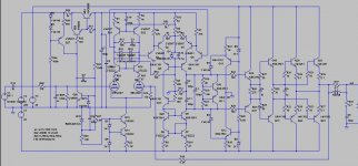
OK guys,
Attached below is a refined version. The I-source load for the LTP did virtually nothing for the overall linearity (they just made up for the little decrease in linearity incurred by the LTP cascodes). THD-20 at 25W into 8 ohms now simulates 0.0015%. However the cascodes will make this version more tollerant of a high impedance source, I guess.
I tried both feed-forward and shunt feedback. The shunt feed back compensation scheme that I ended up using (now slightly revised) actually gave 5 times less THD-20, albiet with a lower slew rate. However, the slew rate is still 75V/us, giving the amplifier a theoretical power bandwidth of nearly 600kHz, so that is hardly a problem.
The design doesn't really lend itself to conventional miller compensation around the VAS, so I didn't bother trying it.
However, like miller compensation, shunt compensation is lag compensation.
I could use a floating LM317 or similar for the +150V supply rail, but I prefer to roll my own.
R15 will be a trimpot (in series with a fixed R) to adjust the bias current.
I put a cascode transistor into the sim for Q5 just for something to do, but I will delete this as it really doesn't do anything usefull. The emitters of the VAS cascode transistors (Q5 & Q6) sit at ~130V, so the extra dissipation in Q5 incurred by the added ~25V won't really matter.
Cheers,
Glen
Cheers,
Glen
Attachments
Hmmm
It appears the part count has increased a bit.
😀
Just a couple quick Q's...
1)Does the swap mirror work (simulate) that much better than the Wilson?
2)Have you had any thoughts on using MOS devices for Q5 & 6?
As a side note, when I made the constant power diff (PNP's with NPN followers, then cascode) I used a complementary matched array ($8 ). This allowed them to be lower Vce devices since there was no collector to GND connection as with the buffered VAS. I could not really tell you if there is much difference in performance, but a lower Vce allows you more component options.
It appears the part count has increased a bit.
😀
Just a couple quick Q's...
1)Does the swap mirror work (simulate) that much better than the Wilson?
2)Have you had any thoughts on using MOS devices for Q5 & 6?
As a side note, when I made the constant power diff (PNP's with NPN followers, then cascode) I used a complementary matched array ($8
). This allowed them to be lower Vce devices since there was no collector to GND connection as with the buffered VAS. I could not really tell you if there is much difference in performance, but a lower Vce allows you more component options.G.Kleinschmidt said:
OK guys,
Attached below is a refined version. The I-source load for the LTP did virtually nothing for the overall linearity (they just made up for the little decrease in linearity incurred by the LTP cascodes). THD-20 at 25W into 8 ohms now simulates 0.0015%. However the cascodes will make this version more tollerant of a high impedance source, I guess.
I tried both feed-forward and shunt feedback. The shunt feed back compensation scheme that I ended up using (now slightly revised) actually gave 5 times less THD-20, albiet with a lower slew rate. However, the slew rate is still 75V/us, giving the amplifier a theoretical power bandwidth of nearly 600kHz, so that is hardly a problem.
The design doesn't really lend itself to conventional miller compensation around the VAS, so I didn't bother trying it.
However, like miller compensation, shunt compensation is lag compensation.
I could use a floating LM317 or similar for the +150V supply rail, but I prefer to roll my own.
R15 will be a trimpot (in series with a fixed R) to adjust the bias current.
I put a cascode transistor into the sim for Q5 just for something to do, but I will delete this as it really doesn't do anything usefull. The emitters of the VAS cascode transistors (Q5 & Q6) sit at ~130V, so the extra dissipation in Q5 incurred by the added ~25V won't really matter.
Cheers,
Glen
Cheers,
Glen
I like your input-load & VAS arrangement a lot. It looks a lot like the one I used in my original MOSFET power amp (different current mirror, though). If you have to go with a unipolar input LTP, I believe this is pretty much the best VAS arrangement. Of course, I used a FET pair instead of the 12AX7.
I had very little trouble with the current mirror phase delay, even in my amplifier where the closed loop bandwidth extended to 2 MHz.
Here's an interesting question. You've included a tube in the VAS and achieved very low THD numbers and wide bandwidth that is the equal or better of many solid state amps. Is there going to really be any discernable "tube sound" lent to this design? If so, why? This is not a criticism, but rather what I consider to be a fascinating question.
Cheers,
Bob
Wow what an amp!😱 Very nice design, congrats! I have a question about it: what is the purpose of Q12 and Q13(along with D3 and D4)?
CBS240 said:Hmmm
It appears the part count has increased a bit.
😀
Just a couple quick Q's...
1)Does the swap mirror work (simulate) that much better than the Wilson?
2)Have you had any thoughts on using MOS devices for Q5 & 6?
As a side note, when I made the constant power diff (PNP's with NPN followers, then cascode) I used a complementary matched array ($8
The 4-BJT mirror only gives a very small improvement in overall linearity. I have to simulate the design at very low output power(~1W) so that the output stage distortion does not mask the input stage / VAS distortion to see it.
I only like to use MOS devices as cascodes for high voltage VAS stages if the dissipation is too high for a high voltage CRT driver transistor. These BJT's still have the edge WRT to transconductance and junction capacitances.
Bob Cordell said:I like your input-load & VAS arrangement a lot. It looks a lot like the one I used in my original MOSFET power amp (different current mirror, though). If you have to go with a unipolar input LTP, I believe this is pretty much the best VAS arrangement. Of course, I used a FET pair instead of the 12AX7.
I picked the biasing voltage off the VAS LTP tail resistor for a larger operating VCE (~10V) on the transistors (incidentally R6 and R7 should be 10k, not 47k). The tail attenuator also ensures less posibility of any AC signal being fed back into the current source transistor bases.
Bob Cordell said:
Here's an interesting question. You've included a tube in the VAS and achieved very low THD numbers and wide bandwidth that is the equal or better of many solid state amps. Is there going to really be any discernable "tube sound" lent to this design? If so, why? This is not a criticism, but rather what I consider to be a fascinating question.
I doubdt it. Maybe if you turn the volume down and tap the 12AX7 with a screwdriver.
emanuel_hr said:Wow what an amp!😱 Very nice design, congrats! I have a question about it: what is the purpose of Q12 and Q13(along with D3 and D4)?
They are a voltage clamp for the VAS to prevent the Wilson current mirror and the NPN predriver from saturating when the amplifier is driven into clipping.
This gives a cleaner clipping recovery.
Cheers,
Glen
Hi Glen
Nice design, congrats ... when do you think the PCB design will be ready?
Question, do you think that there are any cross-talk issue between side of the valve?
noice
🙂
Nice design, congrats ... when do you think the PCB design will be ready?
Question, do you think that there are any cross-talk issue between side of the valve?
noice
🙂
Hi Mr. Kleinschmidt. congratulations on your last two designs the 10A and 25A!
i too was wondering the same things along the lines of Mr. Cordell. I noticed that your THD performance is indeed very impressive, even when compared to pure solid state designs. this is why i don't fully grasp the need for the twin triode in the LTP. im still new, and know very little about tubes, but i thought the purpose of using tubes was to get the even order THD to make the amp sound 'warmer' or something like that. so if this is the case and you have effectively eliminated the 'tube sound' from your design, as evidenced by your awesome THD performance, then why not just use all solid state components?
not criticizing at all, just trying to learn more from the design of a diy-audio master.
thank you.
KLe said:Hi Glen
Nice design, congrats ... when do you think the PCB design will be ready?
Question, do you think that there are any cross-talk issue between side of the valve?
noice
🙂
Not for a while unfortunately. I'm currently doing PCB layouts for about a dozen other projects

My plan is to get them all done, then take annual leave and do 3-4 weeks of constructing electronic stuff.
Dunno about crosstalk between the triodes. In this application I doubdt that there is any of significance.
gain said:Hi Mr. Kleinschmidt. congratulations on your last two designs the 10A and 25A!
i too was wondering the same things along the lines of Mr. Cordell. I noticed that your THD performance is indeed very impressive, even when compared to pure solid state designs. this is why i don't fully grasp the need for the twin triode in the LTP. im still new, and know very little about tubes, but i thought the purpose of using tubes was to get the even order THD to make the amp sound 'warmer' or something like that. so if this is the case and you have effectively eliminated the 'tube sound' from your design, as evidenced by your awesome THD performance, then why not just use all solid state components?
Obsolete Jfet substitute. No, the 12AX7 is just there because it looks cool 🙂 . All solid state becomes boring after a while.
Cheers,
Glen
If the driver voltage is higher than the "power" voltage, why don't only have diodes? I had it in my mosfet amp with 80 V driver voltage and 70 V power voltage. I got a very nice looking clipping behavior.G.Kleinschmidt said:They are a voltage clamp for the VAS to prevent the Wilson current mirror and the NPN predriver from saturating when the amplifier is driven into clipping.
This gives a cleaner clipping recovery.
peranders said:
If the driver voltage is higher than the "power" voltage, why don't only have diodes? I had it in my mosfet amp with 80 V driver voltage and 70 V power voltage. I got a very nice looking clipping behavior.
????????
This is a triple EF BJT-output amp, not a MOSFET-output amp and the driver voltage isn't higher than the "power" voltage.
Cheers,
Glen
I didn't see how the voltages were so IF the driver voltage was higher (like in my mosfet amp)....

I’m sorry, but you’ve lost me. The pre-drivers, drivers and output transistors all share a common pair of supply rails.
The whole purpose of the VAS clamp circuit I have used is to prevent the VAS current mirror and the pre-driver transistors from saturating during clipping.
Cheers,
Glen
Hi Ho
I’m finally getting my act together now with some free
time encroaching, but I've abandoned the K25A before
completing it. I got my hands on a nice pair of heatsinks
and some other bits and pieces and I desire a higher
power amp for a pair of 4-ohm speakers I’m putting together.
I’ve also scrapped the vacuum tube input stage and used
a dual JFET instead (the tube wouldn’t be visible in the
planned enclosure so there is little point).
I also found that Farnell sell the THAT series quad BJT
arrays in the meanwhile, so to make good use of them
the amp has morphed into a fully symmetrical arrangement
just for the hell of it.
Due to the 40W /4 ohm spec and the resultant low voltage
supply rails 10 parallel pairs of MJE1502(8/9) “driver”
transistors are used in the output stage. A glance at the
Ic/fT graphs on the On Semi datasheet will make this choice
apparent.
There are three other boards for the design. These are
discrete +/- 45V regulators for the input stage and VAS
circuitry and a PIC based protection/power-up timer.
A speaker relay external to the main amplifier PCB will be
used. A pair of multiplexed ADC input of the PIC will constantly
monitor the current through a single pair of output devices
(Q55/Q56) and shut the amplifier down under a fault/OL
condition. The PIC will also refuse to enable the speaker
relay and the input un-mute relay if current cannot be sensed
through Q55/Q56 (see Q57-Q60) as a OL detection failsafe.
Slew rate is about 200V/us and the input stage / VAS sims
0.000051% THD-20 with an ideal output stage and conservative
compensation (for a predicted OPS). I don’t have any half decent
models for the MJE15028/MJE15029 devices, so I did not bother
SPICEing the design any further than that – will just have to wait
and see how linear 10 pairs of these are with 2.5A bias soon
after the boards are etched.
Cheers,
Glen
An externally hosted image should be here but it was not working when we last tested it.
- Status
- Not open for further replies.
- Home
- Amplifiers
- Solid State
- The Kleinschmidt 25A