There is no reason why you can't pick off the audio sooner in the chain and amplifiy it as well. Mr. Lightstar does this. 😉
There are normally simple solutions to these problems if you step back and think about it.
-Chris
There are normally simple solutions to these problems if you step back and think about it.
-Chris
Hi Workhorse
Could you post the conceptual sch of your output stage? I don’t understand how you convince 5 parallel switch mosfets to work in linear way.
Could you post the conceptual sch of your output stage? I don’t understand how you convince 5 parallel switch mosfets to work in linear way.
TOINO said:Here is 1 exemple of class-G drived from the output.
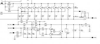
L1, L2, R1, R2, C9 and C10 form two 2nd order filters that prevent the output of the IC to drive the outer stage at high frequencies. It would form a nice oscillator otherwise. Said filters resonate at 200Khz and roll off obove that (assuming a 8 ohm load, as their behaviour is load dependent).
Well, and even in these circumstances, if you study TDA7294 datasheet, you will see that THD is 4 times higher around the power zone where the outer transistors start conducting, and two times higher on average if you compare it to non-class-G plots.
Don't be fooled into thinking that class G does not produce distortion. Anything involving rail switching does.
Hi Eva,
Rail tracking is the preferred method for that very reason.
-Chris
Don't be fooled into thinking that class G does not produce distortion. Anything involving rail switching does.
Rail tracking is the preferred method for that very reason.
-Chris
Ok EVA. Please do not become annoyed!
Every thing that has NFB must be compensated for do not oscillate…
Maybe the important in class-G is the efficiency. Some compromises with THD must be assumed. Otherwise will be impossible to do Kw amplifiers in 2U boxes.
Even if you pick the driver signal before the output stage you steel have some propagation delay in the circuit…and you must handle it in some way…
Optimum is the delay of the class-G driver circuit = delay of amplifier circuit.
Anyway they are solutions for compensate the THD. I remember one BSS amplifier who uses a kind of bridge. One leg is class-H amplifier; the other leg is small voltage amplifier (+/-25V)who just compensates the THD.
And I must agree with Anatech that well done Rail Tracking is the best technical solution, but not the cheaper one.
Well, the point was that you will also get a two-fold or four-fold increase in THD with class G taking the drive signal from the VAS, and class H won't differ much either. It's the rail discontinuity what produces higher THD, and in the end things that look very dissimilar end up being the same 🙂
Sorry but I must disagree...🙁
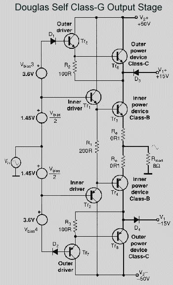
In the Rail Tracking case, the complete circuit is an ideal cascode. Theoretically the THD will be less. With the bonus of no thermal shock on the amplifier transistors crystal.
This shock exists in class-G and is worst in class-H and certainly must influence brutally the “instantaneous THD” of transistors.
Sorry but my English is not enough for this. Sounds like talk about “the sex of the angels”
There is no perfect approach. Even rail tracking has its pitfalls. For example, consider what would happen when the output of the tracking power supply is lagging, say, 20 degrees with respect to the audio signal. Obviously Vce or Vds modulation will happen.
Well, now consider that the amount of lag is speaker current dependent, frequency dependent and level dependent...
Also, consider that the tracking power supply will have sine-shaped output ripple at the switching frequency (say 2V p-p), and that the amplitude of that ripple component may be voltage and current dependent depending on design, thus again modulating Vce or Vds of the linear output stage...
With such complex interactions arising, the only valid way to compare is to design and build the actual circuits and measure their performance and associated waveforms... Do you feel like trying? 🙂
... Do you feel like trying?
Absolutely EVA! Why not? If you do the easy part (switch rail tracking) I will do the remaining!😀
I think that the [motor-driver-amplifier] you talked about in your post 113 is a good start.
Absolutely EVA! Why not? If you do the easy part (switch rail tracking) I will do the remaining!😀
I think that the [motor-driver-amplifier] you talked about in your post 113 is a good start.
I meant if you feel like designing your own tracking power supply from scratch 😀 (you'll probably have to learn SMPS first, as this is an excelent background for switching amplifiers).
Currently I can't since I'm busy completing some very important projects (that actually involve waveform syntesys through switching but that doesn't involve audio at all). However, after completing them I may as well develop three simple reference amplifiers for objective comparison (class G, class H and tracking).
Currently I can't since I'm busy completing some very important projects (that actually involve waveform syntesys through switching but that doesn't involve audio at all). However, after completing them I may as well develop three simple reference amplifiers for objective comparison (class G, class H and tracking).
Absolutely INCORRECT EVA,Eva said:
Also, class H is not a low cost solution because in a proper implementation with controlled slopes the "switching" devices may be subject to considerable dissipation sometimes and should be capable of handling it.
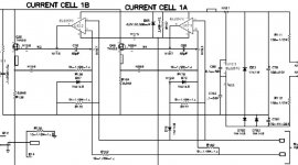
Class-H is low cost than Class-G look at the Schematics of QSC MX2000 and MXA2000 compare them...
MX2000 is Class-G uses 20 Toshiba Transistors per channel ...5 devices in parallel of each Tier + 2 additional driver transistors as well
MXA2000 is Class-H uses 10 Toshiba Transistors per channel ...5 devices for each output half and just 2 low cost Switching IRFZ44N FETs for uper tiers and 2 LM311 low cost comparators...
Class-G is costly as it demands for double the output devices required for class-H....
I think now its clearly evident for you to see that Class-H is low cost than Class-G.....
Switched regards,
K a n w a r😀
Workhorse said:
Absolutely INCORRECT EVA,
Class-H is low cost than Class-G look at the Schematics of QSC MX2000 and MXA2000 compare them...
MX2000 is Class-G uses 20 Toshiba Transistors per channel ...5 devices in parallel of each Tier + 2 additional driver transistors as well
MXA2000 is Class-H uses 10 Toshiba Transistors per channel ...5 devices for each output half and just 2 low cost Switching IRFZ44N FETs for uper tiers and 2 LM311 low cost comparators...
Class-G is costly as it demands for double the output devices required for class-H....
I think now its clearly evident for you to see that Class-H is low cost than Class-G.....
Switched regards,
K a n w a r😀
Don't take existing designs as a dogmatic reference, most are seriously flawed or not optimum in terms of the amount of output transistors employed!
In class G dissipation is *shared* between all devices, when the upper devices are conducting and dissipating the lower ones have a very low Vce across them, and when the lower devices are conducting the higher ones are idle, so in terms of power SOA exactly the same amount of output devices is both valid for class G or class H, as both systems dissipate the same (remember the gentle pulsed ratings that apply for low duty cycles). On the other hand, in class H all devices are always conducting and are all exposed to both high Vce and high Ic (there is not a lower bank that rests when the upper bank kicks in).
Also, don't assume that class H has to be hard switched, I have already explained that soft switching improves it at the expense of increased dissipation in rail switches.
Eva said:
Don't take existing designs as a dogmatic reference, most are seriously flawed or not optimum in terms of the amount of output transistors employed!
In class G dissipation is *shared* between all devices, when the upper devices are conducting and dissipating the lower ones have a very low Vce across them, and when the lower devices are conducting the higher ones are idle, so in terms of power SOA exactly the same amount of output devices is both valid for class G or class H, as both systems dissipate the same (remember the gentle pulsed ratings that apply for low duty cycles). On the other hand, in class H all devices are always conducting and are all exposed to both high Vce and high Ic (there is not a lower bank that rests when the upper bank kicks in).
Also, don't assume that class H has to be hard switched, I have already explained that soft switching improves it at the expense of increased dissipation in rail switches.
I am not taking existing designs as references but just compared them.....in Class-G vs Class-H basis....
If they were not optimum then could you suggest what is more optimum in your view Class-G or Class-H with some reference...
Yes Class-G is exactly what you said...
Cannot agree on the explanation on Class-H by you..
All Devices are conducting....Yes.....
Exposed to High VCE and high Ic simuntaneously ....Correct....to some extent....yes if output voltage crosses upper Tier rail activation Threshold. but at same time doesnot reaches close to the upper rail voltage....in that case its evident to have high VCE and IC at same time.....
Where I have assumed Class-H to be a hard switched phenomena!

Hi Workhorse
“Where I have assumed Class-H to be a hard switched phenomena!”
Both class-G and class-H have hard switch phenomena…
Are you forgetting the switch diodes?? This devices always hard switch.
On your post-133 the D108, who by the way is an Shottky , will hard switch independently of the slew rate of the IGBT.
I think that is exactly here on this diode used in all the amplifiers I have see, that you must work to found an original and glitch free solution.
Why not substitute the diode with a class-G circuit? This way you never have hard switch…
By the way, it seems that you are faster posting others schematics then your own 😀
“Where I have assumed Class-H to be a hard switched phenomena!”
Both class-G and class-H have hard switch phenomena…
Are you forgetting the switch diodes?? This devices always hard switch.
On your post-133 the D108, who by the way is an Shottky
, will hard switch independently of the slew rate of the IGBT.I think that is exactly here on this diode used in all the amplifiers I have see, that you must work to found an original and glitch free solution.
Why not substitute the diode with a class-G circuit? This way you never have hard switch…
By the way, it seems that you are faster posting others schematics then your own 😀
"it seems that you are faster posting others schematics then your own"
I lack the capacity to post original artwork. It is easy to link to prior art to visualize a design point.
At work it takes hours for the technicians to do a schematic capture of a design I can do by hand in a few minutes. Are you saying I should waste my time doing the schematic capture? My employer thinks not, my time costs him more that the technicians' time.
"Why not substitute the diode with a class-G circuit?"
Class G still has a comutating diode.
"Class G still has a comutating diode"
My meaning is that the switching diode is the source of glitches in class-G exactly because it switches…
Forgetting the complexity, why not take it of and put some kind of more linear actuator?
My meaning is that the switching diode is the source of glitches in class-G exactly because it switches…
Forgetting the complexity, why not take it of and put some kind of more linear actuator?
TOINO you seem to forget that the basis of efficiency increase in class G and class H is rail switching. There is no way to implement these circuits without at least diodes (that are among the most elemental switching elements). A switch to disconnect the lower rails while drawing current from whe upper ones is always required.
- Home
- Amplifiers
- Solid State
- The Class - H Amplifier