Stunning performance from a breadboard configuration. Your PCB looks great and should perform even better. I would convert the output to follower config to get 6 more volts of output from the rails.
I get 80w from 40v power rails using 44v regulated vas stage rails.
I get 80w from 40v power rails using 44v regulated vas stage rails.
Dear stocktrader200,
Thank you. I took a good number of days building it. Crucial to me seemed the local feedback loop in the OPS. I've tried many follower outputs. This one tops all in my simulations. I'm okay with the lower efficiency. However I doubt I've tried all followers. Is there a particular arrangement you suggest?
80W from 40V with emitter (or source) follower output I presume?
As for the PCB, I might just order it by the end of this week. I'm considering 6 layer for two extra ground planes. When choosing gold plated pads this is only a small price penalty. However, I should probably not spend as much on what is probably not gonna be the final design. But first I gotta calculate how much parasitic capacity is created by the power planes from critical tracks to small signal ground.
Cheers,
Ruben
Last edited:
H
HAYK
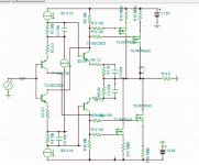
I simulated the OPS. Very clever way using error corrector transistors. I didn't had the models so I used that of KCS/KSA as the driver ones. Biased 230ma I get up to 4W square law class A with distortion 0.0007% at 1W, 0.001% at 5W and above 15W to 150W it remains 0.003%. Such an OPS doesn't require much NFB. If you nest the feedback to drive the OPS by low impedance and apply only 40db NFB, you get ar worst 0.00003% from 15 and up.
I have an auto biased non switching OPS intended to distort 0.3% but opposite phase 3rd harmonics, as the Luxman MQ68C is purposely designed , to subtract the distortion of the loudspeakers. For now it is 0.3% from 200mW to 150W, I will use your "50 years old" technology of IPS, VAS, to get without GFB or with, switchable as Luxman does.
I'll post on separate thread not to polute this.
Dear HAYK,
You can find all the models on Bob Cordell's website. KSA1220/KSC2690 models I got from onsemi which at-least DC-wise are fairly good. The OPS itself forms a simple CFA opamp. Driving it from a high impedance helps the gain margin of the OPS nested FB loop. I will experiment with more degeneration to lower GFB. Slew-rate now is not that high. It is limited by VAS current and by not using degeneration. Some source resistors at the IPS should do.
I look forward to reading about your non-switching auto-bias. Cancellation of speaker distortion is an interesting idea.
Cheers!
Ruben
After some more work on the PCB I believe I am almost there.
Still the top layer hosts most signal traces and 'clean' ground. Bottom is hosting 'dirty' decoupling ground and leftover traces. Inner two layers are positive and negative supply voltages. The two grounds are connected by the output spade connector.
I'm considering the following:
Much cheers,
Ruben


Still the top layer hosts most signal traces and 'clean' ground. Bottom is hosting 'dirty' decoupling ground and leftover traces. Inner two layers are positive and negative supply voltages. The two grounds are connected by the output spade connector.
I'm considering the following:
- Should the shunt compensation capacitor connect to clean ground or decoupling ground?
- Should the current source bias resistor legs connect to clean or to decoupling ground?
- Should the ground-lift resistor separate the entire clean ground or just the input?
- Should the big filter caps and center-tab connect to speaker ground in star-fashion instead of by ground plane?
- Should the feedback network ground have it's own return path or is it fine to connect to clean-ground plane?
- How thick should the output inductor wire be?
- Shouldn't the path from input JFET drains to the active loads be shorter? I feel the front-end layout can be much better.
- Would 6 layer PCB with two extra inner ground planes yield much improvement? With JLC-PCB's gold plated option this would be a small price penalty.
Much cheers,
Ruben
H
HAYK

Post Fuse Electrolytics:
As I realized I was using two 50V caps with 52V rails I swiftly changed them for 100V ones.
Arta showed THD got worse so I removed the caps all together. Measured again and noticed a substantial drop in THD. There were two 220uF caps per rail. One connected close to the OPS and one connected on the way to the front-end. The former helped distortion, the latter worsened it. Removing the caps closer to the vas does reintroduce some ringing:

But THD at 13V7 RMS into 4 ohms is much lower:


Some simulation shows that only 50m Ohm of series resistance caused substantial ripple current through a 220uF elco Almost 6 amps shared over two pieces paralleled which is exceeding the 2.2 Amps ripple current rating of these caps. Respecting the ripple current rating would mean using at-least 3 caps in parallel per rail like on the PCB.
I suspect: On breadboard series supply resistance from the contact points and fuse is much more than 50m ohm, the 6 amps half-ish wave ripple current drops over said resistance, inducing quite some distortion which looks to be mostly even ordered. There is no avoiding a fuse between amp and reservoir caps, so should the post fuse elco's be removed or were they just not routed properly?
Cheers,
Ruben
As I realized I was using two 50V caps with 52V rails I swiftly changed them for 100V ones.
Arta showed THD got worse so I removed the caps all together. Measured again and noticed a substantial drop in THD. There were two 220uF caps per rail. One connected close to the OPS and one connected on the way to the front-end. The former helped distortion, the latter worsened it. Removing the caps closer to the vas does reintroduce some ringing:
But THD at 13V7 RMS into 4 ohms is much lower:
Some simulation shows that only 50m Ohm of series resistance caused substantial ripple current through a 220uF elco Almost 6 amps shared over two pieces paralleled which is exceeding the 2.2 Amps ripple current rating of these caps. Respecting the ripple current rating would mean using at-least 3 caps in parallel per rail like on the PCB.
I suspect: On breadboard series supply resistance from the contact points and fuse is much more than 50m ohm, the 6 amps half-ish wave ripple current drops over said resistance, inducing quite some distortion which looks to be mostly even ordered. There is no avoiding a fuse between amp and reservoir caps, so should the post fuse elco's be removed or were they just not routed properly?
Cheers,
Ruben
Last edited:
H
HAYK
Just a hint. Develop the Amp on two separate PCBs, the OPS on separate. When you need to review one, you don't need to spend time and money for the other part.
For those how like the OPS, or the low level separately, will be able to use it, as me who will use your fabulous "50 year old technology".
,
For those how like the OPS, or the low level separately, will be able to use it, as me who will use your fabulous "50 year old technology".
,
I would give the input section its own RC supply filters. Since the current is small, the capacitors can be small.
Ed
Ed

H
HAYK
I am simulating the Amp without OPS. I was wondering what is the purpose of Q6? No doubt Sansui has done it 50 years ago for my ignorance, it keeps gate drain potential constant inhealing the capacitance effect. I used 2N7000 instead of LKS as I didn't find the spice models. I got 0.0001% for 34vp on the output with 1v input. I replaced the Q11 with 470 ohm resistor and got 0.00003%.
Attachments
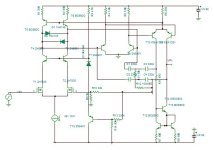
Q6 is the secret sause cascode driver. Wolverine does something similar as it happens. Q11 is used for thermal balance. What sansui amp are we talking about? Would love to have a look at it.
My first amps had seperate front-end pcbs. Was not fond of the extra wiring. I might again but with pinsockets.
My first amps had seperate front-end pcbs. Was not fond of the extra wiring. I might again but with pinsockets.
Last edited:
H
HAYK
It is a fictive Sansui model in the imagination of ostripper, may be Mandalay effect.I doubt that. Distorting ?? WTF. I do concede this 3 stage blows the wolverine away in OLG. In fact , I have the "Kypton" which will be one of my 6
IPS's and is similar to this. This particular IPS dates back to a 1970's Sansui amplifier. Imagine that , the Japanese aced this 50 years ago.
Now , you might have more OLG , but it is the quality of the OPS that allows all that extra feedback to have effect. Bet this amp would have PPM
THD at 50Khz !!
Still , a beautiful topology !
OS
I have seen Pioneer similar but without auto biased CCS with fix common bases.
Where do you see in Wolverine bellow similar to your Q6.
Attachments
Last edited by a moderator:
H
HAYK
To increase the slew rate limit I increased the current of the VAS by reducing the 270 ohm to 100 ohm. It reduced further the distortion to 0.000015%. To balance the dissipation, I replaced the 470ohm with 3.9k but before the comp. capacitor.
Im sure Ostripper does not imagine things.It is a fictive Sansui model in the imagination of ostripper, may be Mandalay effect.
See Q7 on wolverine schematic for similar driven cascode.
H
HAYK
So ask him which model is it. I have never seen any commercial amp using auto biased CCS. There is one on this website I have seen to drive a quasi complimentary 3055. From where you got the idea? I think there is something wrong. I changed the emitter resistors 1.8k, it must act on the open loop gain, nothing is happening. I did remember the Pioneer used NPN 2SC2705, I converted it to use 22k resistors, nothing happened. I will dig in to see why.Im sure Ostripper does not imagine things.
See Q7 on wolverine schematic for similar driven cascode.
Did you build the catharsis with source followers already? Youre fast!I biased mine with a fixed 6.2v zener. The fets are 1rf240 and irfp9140. 55ma of bias is steady
Thank you for the suggestion! I placed 220uF (dont have other values) and 10R RC filter before the front end here are the results driving 4 ohms at 13V7 RMS:I would give the input section its own RC supply filters. Since the current is small, the capacitors can be small.
Ed
- Home
- Amplifiers
- Solid State
- The Catharsis Music Magnifier, The Elusive Hexfet CFP from spice fantasy to PCB