Hi Max,
Good to hear you are getting good results.
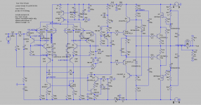
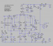
A slightly more elaborated version of the input circuit is shown below.
This should get closer to the JFET version, as each BJT cascode is now driven directly from the emitter signals, and not the common signal from the pair.
Anyway, something to think about and maybe try.
Regards,
Symon
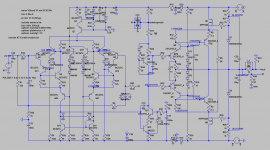
Yes, now that you mention it, what about this other one attached?
The base voltages go up in +/-300mV, though, since the NPNs are now connected to 650mV, instead of 330mV nodes.
Now the input section shall have 12 BJTs instead of only 2... 😀 😀 😀
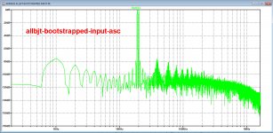
Just for fun I fed it with a 500kHz sine 😎
Thanks for your invaluable contribution to the development of the, soon to become legendary, Amnesis amp, 😀
Cheers,
M.
PS: guys, I think I found Hephaïstos patent. Take a look at it and see if we are missing something cool...
Attachments
Last edited:
If you know me by now, you know my dreams are a VFET bootstrapped output and a Sziklai bootstrapped output. The former is easily done (it only needs courage) but the later is very tricky... 🙁
An example bellow...
Dear Hans, can you please test TIM distortion for our new ALLBJT input?
An example bellow...
Dear Hans, can you please test TIM distortion for our new ALLBJT input?
Attachments
Last edited:
If you know me by now, you know my dreams are a VFET bootstrapped output and a Sziklai bootstrapped output. The former is easily done (it only needs courage) but the later is very tricky... 🙁
An example bellow...
Dear Hans, can you please test TIM distortion for our new ALLBJT input?
Attachments
Dear Max,
I just want to stimulate you, so don't see my comment as criticism.
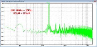
It is quite common that modern high tech amps have a THD20k in the ppm range when loaded with 8 Ohm, see image below as an example: 50Watt into 8Ohm with sub ppm distortion.
For some reason the Amnesis amp does not achieve this, may be because of the very complicated input stage, but it could also be because your Vas is carrying very much current.
And one thing is for sure, low distortion and superb sound reproduction are two different things, but it strikes me as odd that the distortion of the Amnesis Amp is still a bit high for the technology used.
So may be there is still some to be gained.
Hans
I just want to stimulate you, so don't see my comment as criticism.
It is quite common that modern high tech amps have a THD20k in the ppm range when loaded with 8 Ohm, see image below as an example: 50Watt into 8Ohm with sub ppm distortion.
For some reason the Amnesis amp does not achieve this, may be because of the very complicated input stage, but it could also be because your Vas is carrying very much current.
And one thing is for sure, low distortion and superb sound reproduction are two different things, but it strikes me as odd that the distortion of the Amnesis Amp is still a bit high for the technology used.
So may be there is still some to be gained.
Hans
Attachments

Dear Max,
I just want to stimulate you, so don't see my comment as criticism.
It is quite common that modern high tech amps have a THD20k in the ppm range when loaded with 8 Ohm, see image below as an example: 50Watt into 8Ohm with sub ppm distortion.
For some reason the Amnesis amp does not achieve this, may be because of the very complicated input stage, but it could also be because your Vas is carrying very much current.
And one thing is for sure, low distortion and superb sound reproduction are two different things, but it strikes me as odd that the distortion of the Amnesis Amp is still a bit high for the technology used.
So may be there is still some to be gained.
Hans
Dear Hans,
A million thanks for doing these tests for us.

So, the Sziklai is a viable option now. 😎 It is quite complex, though. Edit: I increased IPS current on this one. Did you guys noticed?
Another edit: I should do a JFETinput-Sziklai ouput version which might be superior to this one. 🙂
A piitty that the ALBJT (2nd version) does not perform better. That one has not been tested in real life yet...may I abuse of your generosity and ask for an IMD test for the first version of ALLBJT (being tested now), the one on post n°459, which takes the signal from the common node, before degeneration Rs?? 😱
Edit: Criticism is positive. I don't know why in this post-modern era criticism is viewed as negative, as a personal attack...you are criticizing my(our) project, not my self, which you don't know in person. A critic is "one who knows what is lacking to get a project (or other) to reach perfection", so the function of a critic is very positive and very necessary, safe bad intentions, which cannot be inferred...I am a Virgo, so quite critic and more self-critic myself, hehe.
So do not apologize before formulating a critique, dear Hans.
Yes, I am fully aware of the highish THD from my amp. As I said before "transparency and dynamics" are my goals. Lower THD should impact on transparency but it must not jeopardize dynamics.
As you, I too suspect that VAS is the limiting step. We could search for the ideal current that optimizes both at a time...I think that the raw VAS I am using (an adaptation of DestroyerX's idea) is the culprit of the violence I am experimenting on attacks and which is very welcome. That is one of the reasons why I am reluctant to go into more complex VAS at this point, like your proposed differential VAS, which I am sure can be made to achieve ppm THD but whose dynamic qualities are untested in real life, or the CCS-VAS, whose option will be provided on JOSI's design.
As a fun fact, simulations show 2nd and 3rd harmonic to be at comparable levels, with my obsolete drivers and bootstrap VAS BJTs... 😀
So, at this point, I am privileging dynamics over ultimate refinement, and only decent THD, not to make more technically inclined mates to run away from this interesting project, which has proven so far that COOPERATION is a far better strategy than competition, at least for small communities. The more minds involved the better the potential final result, as has been demonstrated so far. 😎
Cheers,
M.
Last edited:
Some updated circuits optimized for square wave test...
PS: that Hagerman Vbe multiplier surely works as today we have 35°C, the heatsink is hot and the Vbe for the output devices is rock solid.
PS: that Hagerman Vbe multiplier surely works as today we have 35°C, the heatsink is hot and the Vbe for the output devices is rock solid.
Attachments
Last edited:
Dear Max,
I played a bit with your IPS and VAS and achieved these sub ppm distortion figures with simple adjustments.
The red horizontal line is the 1ppm distortion border.
I used only BJT's in the IPS.
Interested what I did ?
Obviously! 😀
Hans
Could it be related, at least in part, to an independent regulated supply for those sections?
Remember we left option to add an external one to be connected on the PS diodes holes.
Thanks very much.
M.
Last edited:
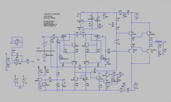
Here it is.
I replaced the OPS by a VCVS, so I could just concentrate on the IPS and the VAS.
The 200uA current source down on the left could be discarded by connecting R6 & R12 directly to V- while changing their value into 400K.
This will slightly increase the 3rd harmonic, that's why.
I hope you can use it and it's again up to you to keep the VAS loading by the OPS low and at the same time to keep the THD under control.
Succes, Hans
Attachments
Here it is.
I replaced the OPS by a VCVS, so I could just concentrate on the IPS and the VAS.
The 200uA current source down on the left could be discarded by connecting R6 & R12 directly to V- while changing their value into 400K.
This will slightly increase the 3rd harmonic, that's why.
I hope you can use it and it's again up to you to keep the VAS loading by the OPS low and at the same time to keep the THD under control.
Succes, Hans
OK. Thanks very much. I will study those mods.
Though at first sight, increasing all 1K resistors for VAS and output to 1K5-2K is very easy to do and test.
As I said before, enhanced EF VAS is very attractive, every time I tried it I got (and this was long time ago, with previous versions) catastrophic oscillation. I will try it again, as time allows, as the present version is much stable. The future PCB shall have provision to this option. Hopefully, the reduced parasitics will make that PCB more stable for everyone to try.
The CCS loaded-VAS version has sort of Hawksford-cascode which is supposed to reduce THD by one order of magnitude...it did not siimulate that way though.
My remembering of the last passive bootstrapped input CFP I tried is not so happy...the active counterparts sound much more engaging though I did not try higher voltages. With a few mods I reduced THD to 1/3 (0.0002%), not ppm I'm affraid... 😱
Cheers,
M.
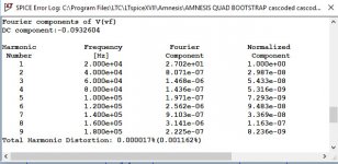
The .asc I sent to you yesterday, still used my bipolar transistors.lib.
I removed that lib and therefore changed the BC550C and BC560C to BC547C and BC557C, the ones that are in the standard LTspice lib.
I also changed the VAS resistors back to 1K each, with no effect on the distortion.
A few additional changes were made: removing the caps from the LEDs in the IPS, and placing a 10pf cap at the minus input.
And the 56p cap on the current mirror was also removed.
To calculate the FFT and the .four command I used a 5msec timeslot. Distortion with .four now reads 0.16ppm.
The only transistor that is not in the standard lib is the BD139C, but you must have this in your amnesis.lib.
So when everything is o.k., you could run the model right away.
Hans
Attachments
Please, remove C8 of 10pF at the minus input.
I was fighting a bug in LTspice, that's how it came there, just to cancel the bug as I found out.
When using the .asc model as I have sent you, you won't experience anything of this bug.
Hans
I was fighting a bug in LTspice, that's how it came there, just to cancel the bug as I found out.
When using the .asc model as I have sent you, you won't experience anything of this bug.
Hans
Dear Max,
I couldn't resist to play a bit further with your Amnesis baby and connected a two stage OPS, using the BJT's selected by you.
I kept it simple, leaving the more complex cascoding up to you, I was just interested in how far the very low distortion of the IPS and VAS could be kept with an OPS driving a real load.
For your information, all test were done with 20Veff@20Khz for 5msec with a timestep of 54 nsec. This output voltage corresponds with 50Watt@8Ohm and 100Watt@4Ohm.
Optimal VAS current for this setting were the two 1K resistors as used by you, and optimal quiescent current in the output stage was 125mA.
When using 4 instead of 2 output transistors, optimal quiescent current dropped to 80mA per pair, but THD dropped hardly, so does this not seem to give any benefit.
And finally I connected an opamp, serving a dual purpose. bringing the output voltage to practically zero volt DC (see below in the image the 0.5mV offset at the output) , but also as an FDR (Feedback Distortion Reduction).
The results are as follows: With the FDR connected, THD was below 1 ppm for all loads between 4 and 16Ohm, a bit depending on the op-amp used.
Without FDR, distortion was a factor 10- 30 higher, mainly being caused by a raised 3rd harmonic.
In real life the THD without FDR will be larger because things are not as nicely matched as in LTspice, but with FDR the real world results will be close to the sim.
Use the info's as you like, I will pull in the background again.
Hans
Attachments
Last edited:
Dear Max,
I couldn't resist to play a bit further with your Amnesis baby Imagine you were actually listening to this baby! and connected a two stage OPS, using the BJT's selected by you.
I kept it simple, leaving the more complex cascoding up to you, I was just interested in how far the very low distortion of the IPS and VAS could be kept with an OPS driving a real load.
For your information, all test were done with 20Veff@20Khz for 5msec with a timestep of 54 nsec. This output voltage corresponds with 50Watt@8Ohm and 100Watt@4Ohm.
Optimal VAS current for this setting were the two 1K resistors as used by you, and optimal quiescent current in the output stage was 125mA.
When using 4 instead of 2 output transistors, optimal quiescent current dropped to 80mA per pair, but THD dropped hardly, so does this not seem to give any benefit.
And finally I connected an opamp, serving a dual purpose. bringing the output voltage to practically zero volt DC (see below in the image the 0.5mV offset at the output) , but also as an FDR (Feedback Distortion Reduction).
The results are as follows: With the FDR connected, THD was below 1 ppm for all loads between 4 and 16Ohm, a bit depending on the op-amp used.
Without FDR, distortion was a factor 10- 30 higher, mainly being caused by a raised 3rd harmonic.
In real life the THD without FDR will be larger because things are not as nicely matched as in LTspice, but with FDR the real world results will be close to the sim.
Use the info's as you like, I will pull in the background again.
Hans
Thanks, dear Hans, for your enthusiasm. 😀 I may become a good salesman someday, probably, hehe.
I have been playing too, as time allows. I want to make compatible your ideas with my experience and I do not want to loose the internal bootstrap for the CFP, which produced a significant sound improvement IMHO. So, I am investigating a mixed approach, a little bit more complex. Probably it has more caps than needed...anyway, I won't be able to make any experiments until a few days...it can reduce THD in one order of magnitude (0,00008%), which is not that bad.
At the end, the burden will be on JOSI1 to design a PCB so elastic and versatile which can handle the most alternative configurations and options as he can. 😀 😱
(at least with connection points for the extra bases of optional BJTs 😉 )
I confess I am a bit suspicious about extra sub-circuits like DC canceling and FDR 🙁
in sonic terms.
Thanks for all the ideas and stimulation.
M.
Attachments
Last edited:
Dear Max,Thanks, dear Hans, for your enthusiasm. 😀 I may become a good salesman someday, probably, hehe.
I have been playing too, as time allows. I want to make compatible your ideas with my experience and I do not want to loose the internal bootstrap for the CFP, which produced a significant sound improvement IMHO. So, I am investigating a mixed approach, a little bit more complex. Probably it has more caps than needed...anyway, I won't be able to make any experiments until a few days...it can reduce THD in one order of magnitude (0,00008%), which is not that bad.
At the end, the burden will be on JOSI1 to design a PCB so elastic and versatile which can handle the most alternative configurations and options as he can. 😀 😱
(at least with connection points for the extra bases of optional BJTs 😉 )
I confess I am a bit suspicious about extra sub-circuits like DC canceling and FDR 🙁
in sonic terms.
Thanks for all the ideas and stimulation.
M.
I'm glad you don't feel annoyed by my suggestions.
If you allow me, a few remarks concerning your answers:
1) In postings on the Audio web, it has been reported by many as almost a surprise how important the contribution of the VAS is in airiness and 3D to the Audio reproduction.
In your VAS things can still very easily be improved, the emitter follower in front of it, the 1000uF connected to the other side of R49 and the different value of R42.
Having done this, you have a top notch VAS that you don't have to pay any attention any more.
Fear for having oscillations has everything to do with the right choice of transistors in the IPS and should be a non issue as the sims are clearly showing.
2) After having an optimal VAS, you can turn your attention to the IPS. As I've mentioned in the past, keep all currents together and don't let audio signals leak away, they are lost forever.
That's why I have taken the emitters of the input transistors as the reference for the cascode transistors and not the GND or a transistor sitting on the emitter line.
Only after the VAS was working in optimal forma, I could reduce the IPS THD by a factor 10 by connecting the LED's directly to the emitters and by using a current source to keep this current constant thereby rejecting the leakage of audio signals.
3) Not wanting to push you in any direction, be aware that just making things that are not working optimally more complex, is never the best way to follow IMHO.
Better is to building step by step on a firm basement.
That also applies to a second cascode in the IPS, a very simple to implement FDR, or whatever possible improvement.
If you don't like it, just remove it, but additional steps should not be made to make the original still improvable design any better. 😀
Hans
Oh Max, one thing that I forgot to tell you.
I used the 2N3904 for the input pair, these are available as duals in one 6 lead SOT package as the MBT3906DW1.
You don't have to match. Temp diff is kept to a minimum and since the sum of the power of both transistors is always the same, you have a very stable temp insensitive solution.
Hans
I used the 2N3904 for the input pair, these are available as duals in one 6 lead SOT package as the MBT3906DW1.
You don't have to match. Temp diff is kept to a minimum and since the sum of the power of both transistors is always the same, you have a very stable temp insensitive solution.
Hans
Dear Max,
I overlooked that in your latest amnesis incarnation you already had added current sources and a VAS emitter follower, great, nice to see.
That made my posting following yours a bit superfluous.
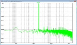
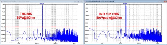
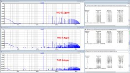
I ran my 20Khz 50Watt@8Ohm test with your latest model, and compared it to what I showed in posting #475, as well without and with the FDR.
Look at the spectra below and the TDH20K figures from .Four next to it.
There could still some mileage to be made as you can see.
I'll have a look at it and come back to you.
Hans
I overlooked that in your latest amnesis incarnation you already had added current sources and a VAS emitter follower, great, nice to see.
That made my posting following yours a bit superfluous.
I ran my 20Khz 50Watt@8Ohm test with your latest model, and compared it to what I showed in posting #475, as well without and with the FDR.
Look at the spectra below and the TDH20K figures from .Four next to it.
There could still some mileage to be made as you can see.
I'll have a look at it and come back to you.
Hans
Attachments
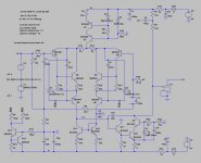
Transistors Q11 and Q12 in your AllBJT model have a Vce=0volt and cannot function as a transistor for that reason.
When increasing their voltage by adding n=2 for D2 and D13, I get oscillations that I cannot tame.
When I replace Q11 ans Q12 by a 2SJ74, gate connected to the bases of the input pair and with enough room to function, things are stable again but THD rises.
With all these interacting transistors in the IPS, you have created a wild horse that will be difficult to tame. 😀
Hans
P.S.1) Q14 and Q16 are still ideal PNP's that should be replaced by real
ones.
P.S.2) I will have a look at the OPS in isolation, coming back on it soon.
- Home
- Amplifiers
- Solid State
- The AMNESIS amp: a good amplifier, like a gentleman, has no memory.