i try to trim the pot for each side and increase voltage on source resistor (0.47R)to approx 0.470-0.500V DC. there is a little different voltage for each R source..
i also measure V AC on 4 parallel output resistor (0.47R) which is 0.015V
V AC accros R source and R ouput are all same 0.019V
If im now wrong AC current gain would be
0.019V /(0.47R/2 ) = 0.08A
0.019V / 0.47 = 0.040A
0.08 / .04 *100% = 50% gain
but bias are very low @ 0.08 x8 = 0.64A / channel
right now it working but the ouput are very low even if i maxed out volume the output are still very low..
i measure DC offset are arround 10-40mV for each channel
Hestsink dimension for 4 IRFP240 are 220mmX250mmX40mm
Hestsink Temp are about 50C with 25C ambient temp
i read on the wiki VAC accross R source and R output should be 0.05V
btw, i use 16.7V toroidal transformer supply rail are about 19-20V DC
anyone can help me how to increase its output?
or maybe i wrong measuring it?
any help would be appreciate..
thank you
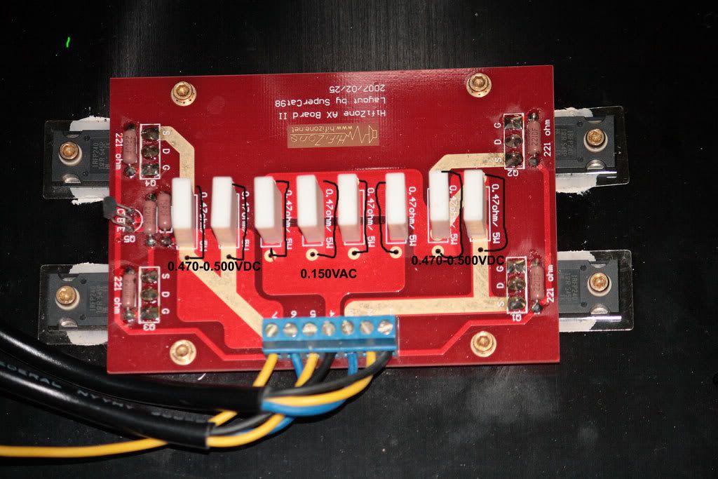
here i attach picture.. the correct V accross ouput resistor are 0.019V not 0.150V.
i also measure V AC on 4 parallel output resistor (0.47R) which is 0.015V
V AC accros R source and R ouput are all same 0.019V
If im now wrong AC current gain would be
0.019V /(0.47R/2 ) = 0.08A
0.019V / 0.47 = 0.040A
0.08 / .04 *100% = 50% gain
but bias are very low @ 0.08 x8 = 0.64A / channel
right now it working but the ouput are very low even if i maxed out volume the output are still very low..
i measure DC offset are arround 10-40mV for each channel
Hestsink dimension for 4 IRFP240 are 220mmX250mmX40mm
Hestsink Temp are about 50C with 25C ambient temp
i read on the wiki VAC accross R source and R output should be 0.05V
btw, i use 16.7V toroidal transformer supply rail are about 19-20V DC
anyone can help me how to increase its output?
or maybe i wrong measuring it?
any help would be appreciate..
thank you
here i attach picture.. the correct V accross ouput resistor are 0.019V not 0.150V.
audioholik said:......
you mixed two things - Iq and AC gain
Iq is quiescent current , also called bias current , and in your case is roughly 1A per mosfet , and that looks good enough to me
AC gain here is gain of Aleph CCS for signal ; when Papa sez 50% , he means that contribution of Aleph CCS in overall AC amplitude is 50% , meaning that upper and lower part of amp have same contribution in amplifying
if you want more help - find schematic of your amp, make some measurings , write (draw) them on schematic and post here
at least for me - it's easier to see on schematic what's wrong , then to re-read several posts to catch what's exact topology of your amp
hi Zen Mod
thank you i have done my homework measuring and routing all my aleph X..
it is supposed to use Kristijan schematic, they are so much a like with a little differences..
im a little confused about measuring voltage wheter its AC or DC..
V AC accross Current source resistor are the same with paralleled Output resistor which is 0.019V AC
(i keep getting random reading with my el cheapo DMM arround 0.011VAC - 0.019VAC, but they are the same V both side when i measure it at the same time)
Voltage Accross Current Source Resistor are about 480mv DC - 500mv DC.. you can see on schematic below for each irfp240
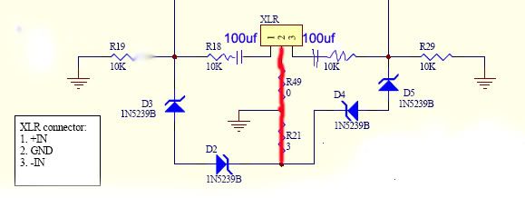
input are like greys sch i see 4 diode's for each channel. but at pin 2 (GND) there no resistor to ground and from ground to diode's. i think they straight go to ground. see my attachment below..
notice big difference in resistor after trimpot original sch say its 75k and in my amp its only 15K..
are there any problem in my amp? becoz i think its output are very low

thank you i have done my homework measuring and routing all my aleph X..
it is supposed to use Kristijan schematic, they are so much a like with a little differences..
im a little confused about measuring voltage wheter its AC or DC..
V AC accross Current source resistor are the same with paralleled Output resistor which is 0.019V AC
(i keep getting random reading with my el cheapo DMM arround 0.011VAC - 0.019VAC, but they are the same V both side when i measure it at the same time)
Voltage Accross Current Source Resistor are about 480mv DC - 500mv DC.. you can see on schematic below for each irfp240
input are like greys sch i see 4 diode's for each channel. but at pin 2 (GND) there no resistor to ground and from ground to diode's. i think they straight go to ground. see my attachment below..
notice big difference in resistor after trimpot original sch say its 75k and in my amp its only 15K..
are there any problem in my amp? becoz i think its output are very low
sorry i forgot..
on input there are 100uf/16v elna bipolar cap in series with 10K resitor..
is it for DC blocking? are there any bad effect to overall performance?
thanks for your help.. and sorry for being such a newb
on input there are 100uf/16v elna bipolar cap in series with 10K resitor..
is it for DC blocking? are there any bad effect to overall performance?
thanks for your help.. and sorry for being such a newb
1. you can't measure AC output above , say, 400Hz with any validity - with cheap DMM
2. if your amp is really made according to that schematic , I can't see anything wrong , and responsible for low gain ;
anyway - you didn't tell in which arrangement you're using that amp - is it in balanced or unbalanced input mode , what is signal source and did you compare it's gain with some other amp?
maybe problem isn't in amp itself , but in something else ;for example - if you are using it with unbalanced signal , and forgot to ground neg input .......
Hi zen,
heres my setup right now
Cayin CDT15A as transport ->TDA1541A NOS DAC - >10K passive attenuator -> Aleph X -> DIY proac 2.5
im using unbalanced input and they are already shorted between GND and -In
correct me if im wrong.. im measuring V AC not DC this time!
right now im using 60hz sinewave with an 8ohm load to measure V AC accross R source resistor (R5 on Grey's) which is 0.033V
and R2/R3 on greys sch which is only 0.010V
from the wiki i read they are supposed to be 0.05..
while now im getting this reading show on blue
from here where do i do wrong
thank you..
audioholik said:when i raise the volume into a little below or normal listening level..that problems seems dont appear on very little volume
All very nice and well, but the soldering of the boards looks like a lousy job, first thing the bloke should do is to reflow all the joints.
The outer edge of the goop surfaces under the IRFs alone makes me puke, goldy-locks screws to hold the boards but zero attention to where it really matters.
Just a single glance at the 1st picture shows half a dozen assembly flaws.
The top center 4-row lytic caps are really hilarious BuTuWu, what did they do, forget the caps during the layout design ?<= 2nd part to check !
3d : the various garbage connector blocks.
audioholik said:i have some problems with my alephX..
What are the DC voltages at +out and -out, referenced to earth?
Also the DC voltages top and bottom of every 9610.
I would double check that the input wiring is correctly wired as unbalanced.
I also suggest you try it with balanced input before going any further.
tnargs said:
What are the DC voltages at +out and -out, referenced to earth?
Also the DC voltages top and bottom of every 9610.
I would double check that the input wiring is correctly wired as unbalanced.
I also suggest you try it with balanced input before going any further.
lol, absolute DC voltage are about 5V... now that you mention it.. i adjust it to about 200mV after 1 hour running..
now, it have more power to drive my proac clone and yess of cource a lot better low extension..
i should thank and pray for you

1 or more thing, are there any bad effect to have difference Voltage @each source resistor ? i measure the lowest are 470mv and the highest are 510mv..
here's my last measuring for 1 channel
last , what will happen if i remove those 4 caps right @ the input? they are bipolar 100uf lytics.
will it raise my diff dc offset if i remove it?
now i have <50mv DC offset both channel..
thank you
1 or more thing, are there any bad effect to have difference Voltage @each source resistor ? i measure the lowest are 470mv and the highest are 510mv..
Probably due to your output devices not being matched very closely.
Anthony
...are there any bad effect to have difference Voltage @each source resistor ? i measure the lowest are 470mv and the highest are 510mv..
Coulomb said:Probably due to your output devices not being matched very closely.
Yes, not a real concern in terms getting your amp to work. But of course the X-effect (distortion cancellation) depends on the exactness of the match of the devices. See wiki.
Also see wiki http://www.diyaudio.com/wiki/index.php?page=Aleph-X section 4.5 for discussion of your question: removal of input coupling capacitors.
Su-Sy with unbalanced input?
The above discussion of Coulomb's unbalanced-input Aleph-X leads me to ask a question of the group:
Is the super-symmetrical circuit still cancelling distortion as effectively if an Aleph-X is running an unbalanced input, compared to balanced input?
I had assumed that Su-Sy operation needed balanced input. And that to run the amp "in Su-Sy" with an unbalanced input required an unbal-bal converter between the rca plug and the XLR input wiring. I came to this conclusion after reading Nelson's article on Su-Sy here http://www.passdiy.com/pdf/articles/susy.pdf, which says "Su-Sy is an approach that takes advantage of balanced operation like no other design, and requires a balanced input to retain the precisely matched behaviour. You can drive one input alone, and the circuit will amplify reasonably well, but it will not exhibit the very low distortion character of fully balanced operation."
Hence my suggestion to Coulomb that he try using balanced input, and soon. I am surprised that anyone would want to run a Su-Sy amp with unbalanced inputs, forfeiting the whole advantage of the circuit! Yet the wiki is strangely silent on this point. Am I wrong?
Re: Su-Sy with unbalanced input?
sorry, I meant audioholik, not Coulomb!!
tnargs said:The above discussion of Coulomb's unbalanced-input Aleph-X .....
sorry, I meant audioholik, not Coulomb!!
Was a hard job digging out this thread !!
Someone ask at the Solid State forum about my balanced protection circuit :
http://www.diyaudio.com/forums/showthread.php?postid=1656907#post1656907
&&&&&&&&&&&&&&&&&&&&&&&&&&&&&&&&&&&&&&&&
Patrick,
Abot absolute DC offset and speaker protection on aleph-x...
I found this for balanced speaker protection circuit on aleph-x thread. IF this operate when absolute DC offset several volts,
I mean that realy is on position at high absolute DC offset...
I have to use this circuit. But I can't read exact zener value and constant current IC. Please let me know.
Regards,
Chois
&&&&&&&&&&&&&&&&&&&&&&&&&&&&&&&&&&&&&&&&
Here are the answers :
The J508 is a constant current diode at 2mA. So under normal operation, each leg of the diff pair will get 1mA, anf that means 2V across the 2k resistors. To trip the relay, you need say 0.65V at the base of the BC550C. That means (0.65V Vb + 3.3V Zener + 0.65V IN4148) = 4.6V at any one of the 2k resistors. The gain of the diff pair itself is (2k/1k)=2, but then I have 2x 100k potential divider between the input and the base of BC640, so the total gain is 1. That means that the trip voltage will be (4.6V-2V) = 2.6V, or thereabouts, depending on component tolerances.
To change the trip point, you can either change the 3.3V Zener diode (changing to a higher value say 3.9V will lower the trip point by 0.6V), or change both the 2k resistors (higher value will lower the trip point).
Hope it is clear.
Patrick
Earlier in this thread, the two Ians were discussing the sonic signatures of the various IRFP N-FETs. I built my Aleph-X on the hifizen boards with the 150N because of its excellent transconductance to gate capacitance ratio. If Nelson is using that many FETs he must be grouping them in a way (ie: serially) to either reduce their cumulative gate capacitance or take that capacitance effect out of the circuit. I only used the 4 parts on that board and biased them hard with 250 milliohm source resistors and 20V rails primarily with the hope that I would be able to achieve cleaner, lusher highs but I failed. After hearing other builds I can tell you that my amp seemed to have a better bottom and more control when untattenuated but there was a lack of flair on the top. Nelson had hinted that a JFET front end would probably open up the highs by reducing some gain. He also stated that the fewer the number of FETs the greater the importance of matching becomes and matching not only for working (settled) transconductance but also for transconductance profile (ie: speed to settled transconductance). He also said the layout would have more importance on noise cancelling in the high frequencies. I didn't have time to read everything after reading Ian McMillan's effort so forgive me if this information provides limited utility.
I'm not clear what you mean when you say Nelson's grouping MOSFETs 'serially' to reduce capacitance. The output stage is what it is. The more devices in parallel, the more Gate capacitance you'll have to drive. You could cascode the output stage (something I considered doing at one point but never followed up on) to reduce the effect of the capacitance, but that's about it.
I'm also having trouble following what you mean about matching becoming more important with fewer devices. It should be the other way around.
Obviously, the choice of MOSFETs influences the overall sound. If you want a lighter, more open, sound, go for MOSFETs with less Gate capacitance (all things being equal). Changing the front end to JFETs will be somewhat more problematic. The transconductance will be lower than the IRF9610s, which will lower the open loop gain of the amp and hence the amount of negative feedback. This can be argued either way; it depends on what you mean by 'cleaner, lusher highs.' I've spent a lot of time in the last couple of years trying to get decent performance out of circuits with as little feedback as possible. To me, the idea of less NFB is a good thing. Others like the sound of more feedback. Overall, a lower feedback amp tends to have softer, less aggressive highs. That may or may not be what you're searching for.
Given that you say you've heard other Aleph-Xs that sounded better, I'd say your path is clear...pull the output MOSFETs and replace them with something less hefty. If I'm recalling correctly where the 150 fits in the overall scheme of things, you chose a 'darker' sounding MOSFET, but that doesn't mean you can't adjust things now that you've heard the result.
Grey
EDIT: Actually, given that JFETs wouldn't be a drop-in replacement, you're free to put together a front end with about the same gain as the MOSFET one. The problem you'll run into is that the JFETs won't be able to take as much bias current, which will have implications as to how well they can drive a given output stage.
Grey
The tolerance needs to be tighter for fewer devices. When there are many devices, the load drive is 'averaged' better. A 20mV difference between the two mosfets in my amp would be much less symmetrical than that same 20mV difference shared over eight FETs. What exactly makes the 150N part darker? Looking at the spec sheets, I can not understand what makes it 'darker' than the 044 part. I have assumed that my layout is not taking full advantage of the noise cancelling characteristics in the upper frequencies more than my choice of 150N parts, am I wrong?
The tolerance needs to be tighter for fewer devices. When there are many devices, the load drive is 'averaged' better. A 20mV difference between the two mosfets in my amp would be much less symmetrical than that same 20mV difference shared over eight FETs. What exactly makes the 150N part darker? Looking at the spec sheets, I can not understand what makes it 'darker' than the 044 part. I have assumed that my layout is not taking full advantage of the noise cancelling characteristics in the upper frequencies more than my choice of 150N parts, am I wrong?
Methinks your reasoning regarding matching is skewed. Look at it this way, if you go to the irreducible minimum of one, there's nothing to match with and you have complete freedom to use any Vgs you choose.
Who says the '044 isn't dark? It is, comparatively speaking. Go for something lighter.
Grey
Who says the '044 isn't dark? It is, comparatively speaking. Go for something lighter.
Grey
"darkness" is totally in the context of the rest of the circuit. None of these
Mosfets are dark of themselves.
The issue of using Jfets as drop in replacements is easier to do if you have
lots of them. At PL we have had some designs in which we paralleled
2SJ109's to get the transconductance and bias figures we wanted.
😎
Mosfets are dark of themselves.
The issue of using Jfets as drop in replacements is easier to do if you have
lots of them. At PL we have had some designs in which we paralleled
2SJ109's to get the transconductance and bias figures we wanted.
😎
- Home
- Amplifiers
- Pass Labs
- The Aleph-X