Hi mp8. Welcome aboard.
I've got a schematic and a layout going. I will post the schematic once I get it finalized. Then I'll post my layout and you guys can criticize it all you want 😉 It's working out pretty well so far. I'm nitpicking a bit over the grounding connections, which takes a little time. There are still some things I need to add on the input side and a capacitor for the snubbers on the output side. All the major components have been selected though. It's more of an issue to figure out what package to use for some of the parts that have to be added. Eagle makes you define the part with a certain package in the schematic and won't let you change it in the layout, so you have to know what you're using before you place it. Sometimes that's a little counterproductive if you want to work on the layout but don't know exactly which footprint you'll be using, but it really does help you to get your act together and get organized when doing schematics and layouts. I wish the company I worked for did this...
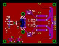
Here's what the board looks like now. There are about 30 airwires left. Notice how all the through hole components are on the opposite side of the board. This was done so you can attach the TAS5261 heat slug to a large heatsink or a metal case while allowing the electrolytic caps to be placed as close as possible to the chip's power pins.
I've got a schematic and a layout going. I will post the schematic once I get it finalized. Then I'll post my layout and you guys can criticize it all you want 😉 It's working out pretty well so far. I'm nitpicking a bit over the grounding connections, which takes a little time. There are still some things I need to add on the input side and a capacitor for the snubbers on the output side. All the major components have been selected though. It's more of an issue to figure out what package to use for some of the parts that have to be added. Eagle makes you define the part with a certain package in the schematic and won't let you change it in the layout, so you have to know what you're using before you place it. Sometimes that's a little counterproductive if you want to work on the layout but don't know exactly which footprint you'll be using, but it really does help you to get your act together and get organized when doing schematics and layouts. I wish the company I worked for did this...
Here's what the board looks like now. There are about 30 airwires left. Notice how all the through hole components are on the opposite side of the board. This was done so you can attach the TAS5261 heat slug to a large heatsink or a metal case while allowing the electrolytic caps to be placed as close as possible to the chip's power pins.
Attachments
You get to pick what you use, but there's room for T106 size cores. The holes should be able to fit up to 14ga wire.

Hi Brian
very nice job.
if you lookat the TAS5261 PCB layout at www.ti.com a litle closer, the GND plane is attached directly to the GND pins on the device - this is a must to get the device working.
The GND plane is the best return path of all the switching.
It also seems that your decoupling caps the 1000uF gnd are not connected directly to the GND plane - also important.
The gerber files for the TI layout is avaiable on http://focus.ti.com/docs/prod/folders/print/tas5261.html
If you look at page 16 in http://focus.ti.com/analog/docs/techdocsabstract.tsp?familyId=922&abstractName=slaa332
there are some placement notes for the components around the TAS5261
rgds,
Kim

kims said:if you lookat the TAS5261 PCB layout at www.ti.com a litle closer, the GND plane is attached directly to the GND pins on the device - this is a must to get the device working.
The GND plane is the best return path of all the switching.
It also seems that your decoupling caps the 1000uF gnd are not connected directly to the GND plane - also important.
The gerber files for the TI layout is avaiable on http://focus.ti.com/docs/prod/folders/print/tas5261.html
Hi Kim. Thanks for taking the time to look some of this stuff over. I've already viewed both the TAS5261 datasheet and evaluation board pdf files in detail and have read their placement notes and looked over their evaluation board layout. Why start completely from scratch when they've already done some of the work, right? 🙂 Especially when they already have a proven design.
In my layout the ground plane is only used for sensing analog ground and for shielding. The power grounds have their own returns which keep the high currents out of the ground plane. It is true that the output power ground must also be connected to the analog ground, and it should only be done at one point. I have not yet decided where I want to do that, which you so astutely noticed 🙂 In this circuit, there are four separate grounds that need to be somehow connected: 3.3V power ground (analog ground), 12V power ground, and the output stage power grounds (one for each mosfet half bridge). The output stage grounds will be tied together and to the 12V power ground at one point and that will then be tied to the analog ground at one point. The "point" connections will be done with 0 ohm jumper resistors or you can just short out the pads. That way, if there does happen to be a ground issue you could try a low value resistor in place of the jumper.
Another thing I'd like to point out is the reason I chose to derive the 12V gate supplies from the output power stage rail while using a separate external supply for the other 12V section. Power for the gate drive supplies will be drawn from the output rail and returned directly to the output power ground instead of the separate 12V supply ground. We want to keep all of the high current out of the ground plane so it can actually be used as a ground reference and for shielding purposes. However, as Kim correctly pointed out, the output power ground must be connected to the other ground for the circuit to work properly. The best way to connect them is at one point so you can avoid ground loops and high currents flowing through the ground plane.
The more complicated the circuit gets the harder it becomes to give each component its own return path to ground. That's why you see a lot of designs that have everything connected to a ground plane without giving it a second thought. This circuit isn't too complicated but still requires careful attention to these issues.
Hi Brian
Star grounding only works with analog circuits - here you have a high voltage/current switching circuit - use one solid GND plane and connect all GND pins and parts directly to the GND plane. Thats what works with the TASxxxx parts.
rgds,
Kim
Star grounding only works with analog circuits - here you have a high voltage/current switching circuit - use one solid GND plane and connect all GND pins and parts directly to the GND plane. Thats what works with the TASxxxx parts.
rgds,
Kim
kims said:Star grounding only works with analog circuits - here you have a high voltage/current switching circuit - use one solid GND plane and connect all GND pins and parts directly to the GND plane. Thats what works with the TASxxxx parts.
Hi Kim. That is not completely true, but then again this circuit is all analog and will be operating around 250kHz. You do not have to connect all ground connections to one solid ground plane. In fact, that may end up causing more problems by creating loops if the component placement isn't very good. The only high voltage, high current part of the circuit is the output half bridges and their supply pins are isolated from the rest of the circuitry. The output power ground still needs to be connected to the other grounds on the PCB (because the ground pins are isolated on the package), but the power and return traces may be separate from each other and the ground plane to ensure that the high currents flow where you want them to - i.e. not the ground plane that will be for analog ground.
Hi Brian
I / We have solid experience with GND planes and the TAS5261, and that is simply what works - you are welcome to do it differently - but then expect to see problems/issues
rgds,
Kim
I / We have solid experience with GND planes and the TAS5261, and that is simply what works - you are welcome to do it differently - but then expect to see problems/issues
rgds,
Kim
Hi Kim. I didn't know you had experience with this particular TI chip since it's so new. Has your design for this chip been implemented in any products or is it for personal use? I'm just curious 🙂
I'm sure you've noticed that the TAS5261 eval board uses a 3.3ohm ground lift resistor between the analog ground and the power ground. You know they do that to try and isolate the analog ground from the dirty ground plane. You wouldn't need any resistor (which is the best option) if the high currents were kept out of the ground plane.
I'm not saying TI's layout is bad, because it clearly isn't, but you don't need to have all ground connections made directly to a ground plane for this "digital" circuit to work well. However, you do need to know where the high currents will be flowing and provide an adequate path for them.
Jaka, thanks for those links! I had no idea Kim worked for TI 
Kim - can you provide any details as to the exact connections of the ground and power pins internal to the TAS5261? The datasheet explicity states that the power and ground pins for the half bridges are completely separate from each other, but what about the other power and ground pins? Pins 8 and 16 are designated power ground in the datasheet - are they the ground points for the circuitry powered by 12V Vdd, including the gate supplies? There is also an internal 3.3V regulator that draws power from the Vdd supply, correct? I would imagine the analog ground (pin 9) is the ground pin for the 3.3V supply electronics only. I would also imagine that none of the ground pins are connected internally, and as such they must be connected externally as is shown in the schematics. Is that true?
Any other interesting things you could possibly share with us about this fascinating chip? Finally, thank you for stopping by this thread. It's always nice to see someone like yourself (who works for the manufacturer) interested in the DIY side of things.
Hi Kims, and thanks for stopping by. I too would be interested in any comments you have regarding optimum implementation, especially Brian's idea of using the TPA2000D1 as a PWM front end.
pinkmouse said:especially Brian's idea of using the TPA2000D1 as a PWM front end.
Yes, that too 🙂 Also, any ideas for another front end capable of PWM output (preferably one that has a 50% duty cycle PWM signal at idle) that's comparable in simplicity to the TPA2000D (2W version) or TPA2001D (1W version) would be most welcomed!
I've got some ideas kicking around that involve incorporating the MP7720 chip I use on my D10.1 modules with the TAS5261 to make a rather powerful self oscillating amp.
The 3.3 Ohm resistor serves a special purpose. It helps to keep the device operating smoothly at high power levels (Kim may not be the only TI employee lurking around).
In general the best practice for these amplifiers is as Kim stated, one large ground plane.
In general the best practice for these amplifiers is as Kim stated, one large ground plane.
BWRX said:... to make a rather powerful self oscillating amp.
It may just be my analogue heritage, but I find that phrase very uncomfortable! 😉
- Status
- Not open for further replies.
- Home
- Amplifiers
- Class D
- Texas Instruments TAS5261