I got a stereo dual chip 2x420=840 watts Tda8954th amplifier board with adual 24 500va (watts)Transformer. In the circuit board those to chip has 2 individual 10amps bridge rectifiers for 2 individual power supply. I'm not sure the max current rating for the IC but date sheet mention somewhere current rate should not be over 12amps I could be wrong. Datasheet also mentioned btL mode 8ohm load 420watts. My questions are how am I supposed to get 420+420=840watts from a 500watts Transformer? I believe those two chips of tda8954th can't handle 1000va or about 21amps in a 48vac Transformer. But nxp claim btL mode max power outage 420watss. My second question is can I or should I use 4ohm load in it? With a 4ohm load I should be able to get about 600+ watts per btL channel. Am I right.
1. search...😉
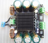
TDA8954TH - XH-M252 board - anyone?
2. pic or link of that board would be nice...
3. i do not believe that you really need 500w-800W...in the datasheet often are values about THD of 10% = for boom box ok for home listening look at 1% THD --< marketing
4. a 24V 500VA trafo has a current of ... 500VA/24V = 20,3A --> diveded per 2 because of 2 windings at out is 10 amps current per output winding...losses not calculated !
5. 420watt with an efficency of class D about 90% means 40W losses on the heatsink !!!!!! --so you need an heatsink like an class a amp !!!---no way
Last edited:
In eBay you will get it with pictures. I don't have it on me now. Thank you
420w x 2 ac 24v tda8954th dual-core digital audio amplifier board with cpu fan hifi two channel amplifier Sale - Banggood.com
?
Neue 420 watt x 2 AC 24 v TDA8954TH dual core Digital power Verstarker 2,0 dual kanal audio Verstarker Bord mit zwei fan B8 005 in Neue 420 watt x 2 AC 24 v TDA8954TH dual core Digital power Verstarker 2,0 dual kanal audio Verstarker Bord mit zwei fan B8-005 aus Verstarker auf AliExpress.com | Alibaba Group
an russian guy did some test...its not my language 😀
https://www.youtube.com/watch?v=olo_YVLJJMw
at 14:34 you will see the result
https://www.youtube.com/watch?v=olo_YVLJJMw
at 14:34 you will see the result
I got a stereo dual chip 2x420=840 watts Tda8954th amplifier board with adual 24 500va (watts)Transformer. In the circuit board those to chip has 2 individual 10amps bridge rectifiers for 2 individual power supply. I'm not sure the max current rating for the IC but date sheet mention somewhere current rate should not be over 12amps I could be wrong. Datasheet also mentioned btL mode 8ohm load 420watts. My questions are how am I supposed to get 420+420=840watts from a 500watts Transformer? I believe those two chips of tda8954th can't handle 1000va or about 21amps in a 48vac Transformer. But nxp claim btL mode max power outage 420watss. My second question is can I or should I use 4ohm load in it? With a 4ohm load I should be able to get about 600+ watts per btL channel. Am I right.
HI Shovon,
ST specifies 420W output (BTL) because it sounds impressive and many have a "blind focus" on power. When ST claims such an output power it is no-doubt true but it may be under laboratory conditions with a water-cooled heatsink and PCB-tracks of unusual thickness.
Your board is produced as a low cost product, most likely according to ordinary standards and with an ordinary heatsink. The manufacturers normally take over the specifications from the datasheet without further consideration if their implementation will allow for the full datasheet potential.
As engineers we have the possibility to perform a critical review of the stated performance.
For such super-high power single chip amplifiers two issues are of particular interest: cooling and current handling.
Cooling: The TDA8954 chip is delivered in two housings, one for SMD mounting and one for "through hole" mounting. I have both. The "through hole" mounting version allows for much better cooling than the SMD version. Your board no-doubt uses the SMD version. The ST specifications may be based on the "through hole" version. The SMD housing has got a small metallic cooling pad to be put in contact with the heatsink. When evaluating such power specifications, a first very relevant approach is by estimating the heat-loss in the chip that has to be removed by the heatsink. 420W output with an efficiency around 90% leaves 44W to be cooled off the chip. With the SMD housing that seems to be very difficult. For the "through hole" version it will be delicate but possible with care. If you, as you suggest, use a 4 Ohm load and get 600W out, it will be 66W to cool off the chip. This first consideration leaves an impression that even 420W continuous power is hardly possible.
Current: Just as a very rough comparison we, here in Europe, use 1.5mm2 copper to handle 10A current for lighting in our houses. That is with a lot of margin. But, try anyway to compare 1.5mm2 with the amount of copper you have available for the pads and tracks near the tiny chip leads. At least we start doubting if this is possible on a more permanent basis for the SMD version. For the "through hole" version it may be different. Your board most likely uses standard copper-foil thickness.
On top of these considerations you have a point where the current limitation in the chip kicks-in. Remember, that is normally specified as the peak value.
Since the old HiFi-norm (DIN45500 in Europe), output power is measured continuously where heating is relevant. Your board may be able to supply 420W for a short moment where the heat capacities can still handle the short moment of power. I have strong doubt about 420W continuously. The 420W claimed for your board could conveniently be interpreted as 420W "dynamic power".
As I understand, you use a 500VA transformer. Evidently, that will not give 2x420W continuous output. But for music, you have a crest-factor indicating that you only need to design (statically) for less than half of the maximum dynamic output power. 500VA is a good choice for an amplifier used for music.
My conclusion: 2x420W continuously is impossible among other because of your transformer. The possibilities for you to modify your construction to get 2x420W continuously are very small and practically futile. You may have 2x420W dynamic power relying on the storage capacitors and that should be enough to harm your hearing long term.
Last edited:
So I ordered a 1000va Transformer for it. My concern is I bought 2 600 pick watt 8" speakers (400 rms). Does speaker's has really 600watts? I wanted to by something like (load) 20% less than my amplifier's output.
So I ordered a 1000va Transformer for it. My concern is I bought 2 600 pick watt 8" speakers (400 rms). Does speaker's has really 600watts? I wanted to by something like (load) 20% less than my amplifier's output.
An 8 Inch speaker exposed to music with near 400 Wrms of power, I dare not think of the result. With reasonable speaker efficiency the movement (stroke) should be enormous. My feeling is "no way". I have no experience with high power speaker units.
So I ordered a 1000va Transformer for it. My concern is I bought 2 600 pick watt 8" speakers (400 rms). Does speaker's has really 600watts? I wanted to by something like (load) 20% less than my amplifier's output.
Hi shovon
Please read 4 -5 times the statment of FF...... and then think about once again.
i wrote you very short ....plus FF give you an detailed explanation how to calculate in detail what happend at a chip....real condition...lab conditions
what happend on some pcb=board....etc...
believe us you do not get such a power from this amp !!!
chris
how to calculate a PSu for Class D
Here is a very very very good statement of FF about PSU:
i did not note the page but maybe a moderator can stick this excellent assumption at the top of all threat in class D forum.
How to choose the power supply for your class D amplifier module.
Typically less experienced DIYs repeatedly ask about this issue. It is not particularly difficult but requires knowledge of Ohms Law, the functioning of a class D amplifier and a Buck (step-down) power converter and some general electronic overview.
Only one channel (mono) will be considered. If you need two amplifiers (stereo) to operate from the same power supply, you simply double the current capability of the power supply such that also the power rating is doubled.
Important parameters
For deciding the right power supply, the maximum (operational) power supply voltage and the maximum output current (where the over-current protection is activated) of the amplifier need to be known (see the specifications or the chip datasheet). You also need to know if the amplifier operates from a single supply voltage or two symmetrical (+ and -) supply voltages. Next, you have to design for optimum operation with 8 Ohm or 4 Ohm speakers, eventually 2 Ohm speakers for automotive use.
The effective operating voltage
The effective operating voltage (Veff) is the voltage the amplifier can use to generate a sine half-wave.
For class D amplifiers operating in BTL configuration from a single supply voltage it is the single rail-to-ground voltage.
For class D amplifiers operating in SE mode with one speaker terminal connected to ground and a symmetrical supply voltage it is the voltage from one rail to ground.
For class D amplifiers operating in BTL mode with a symmetrical supply voltage it is the voltage from one rail to the other rail, thus, double the voltage from one rail to ground.
This effective operating voltage indicates the maximum peak voltage the amplifier can generate for a sine half-wave. From a sine half-wave peak value to the rms value, the factor 1.41 applies. The rms value is found by dividing the peak value with 1.41.
Though the theoretical conversion factor is 1.41, it is suggested to use the factor of 1.5 when calculating the rms value of a sine half-wave that can be generated from an effective operating voltage (Veff). Then, some output switch drop is taken into account.
As an example, for a BTL-coupled amplifier that can handle a single supply voltage of 36V, the rms value of the sine half-wave that can be generated by the amplifier is 36Veff/1.5=24Vrms.
With the rms voltage of the sine wave signal, the power in a load can be calculated using the expression Vrms*Vrms/Rload. Using the values from the example above: 24Vrms x 24Vrms / 8 Ohm = 72W. Or, for a 4 Ohm load: 24Vrms x 24Vrms / 4 Ohm = 144W.
This way we can calculate how much AC signal power it is possible for the amplifier to generate in the load PROVIDED the amplifier can stand the resulting current.
The maximum current for an amplifier output
This value is more difficult to find in a chip datasheet. Sometimes it is specified as the (peak) current the amplifier can handle at an output, sometimes as the output current where the (over-) current limiter is invoked. Some datasheets are not clear about if the chip can stand the maximum (peak) current on more outputs at the same time.
When we have calculated the maximum output power the supply voltage will allow, we have to compare the resulting current against the maximum current for the amplifier chip. To calculate the maximum peak output current, we simply divide Veff with the load impedance. Veff / 8 ohm for 8 Ohm load and Veff / 4 Ohm for 4 Ohm load.
Using the values from the example above, the peak current value in 8 Ohm will be 36Veff / 8 Ohm = 4.5 Apeak. In 4 Ohm it will be 36Veff / 4 Ohm = 9 Apeak. Let’s assume the amplifier can handle 6 Apeak at the output(s), operation with 8 Ohm load is fine (max. 4.5Apeak) but operation with 4 Ohm load (max. 9Apeak) will result in over-current at a certain output level.
If we know we will use the amplifier from the example above with 4 Ohm speakers, we need to lower the supply voltage (Veff) such that the maximum current at an amplifier output is not exceeded. Reducing the supply voltage (Veff) to 24V means the peak current in 4 Ohm will be 6A and the amplifier maximum current is not exceeded.
Calculating the power supply capacity
When the maximum output power that is possible with a certain supply voltage has been calculated and the maximum current at the amplifier output has been successfully checked, we need to calculate the power capacity of the power supply.
Here, we use the knowledge that a class D amplifier has an efficiency of typically 90%. To be prudent we use 80%.
The classical way assuming test with a constant amplitude sine-wave: The maximum output power from the amplifier is divided by 0.8 (80%) to take amplifier losses into account. Using the values from the example above, 72W in 8 Ohm requires a power supply of 72W / 0.8 = 90W. In 4 Ohm, 144W / 0.8 = 180W.
The realistic way assuming use with music: The power supply capacity (Watt) calculated above is divided by two. Why? Because music has got a “crest-factor” meaning that no music is demanding full power for long. Actually, most music has long passages with rather quiet sound and short passages with powerful sound. Therefore, it is seen as unrealistic to design the power supply for maximum sound level all the time. Clever and competent people estimate the steady-state power supply need to be half of what is normally needed for the maximum power the amplifier can output. The power line decoupling capacitors are handling the need for short but powerful surge currents.
Using the example above with 72W in 8 Ohm will then require only a 45W power supply (half of 90W).
Can we swap 4 and 8 Ohm loads?
Yes, but with two different results. If the amplifier and power supply are optimized (designed) for a 4 Ohm load, you can always use an 8 Ohm load instead – but, you will only get half the output power. No overload. If the amplifier and power supply are optimized for an 8 Ohm load, you can use a 4 Ohm load instead at lower output levels. But at a certain output level, the higher current demanded by the 4 Ohm load will exceed the current capability of the amplifier and perhaps also power supply such that you have an over-current situation.
Therefore, 8 Ohm speakers are the most versatile if you do not need the extra power.
An 8 Inch speaker exposed to music with near 400 Wrms of power, I dare not think of the result. With reasonable speaker efficiency the movement (stroke) should be enormous. My feeling is "no way". I have no experience with high power speaker units.
the linear movemente is written in some serious datasheet of the speaker...after this you get non linear movement of the membran --> its not linear and the membran is tweaking --> more distortion ---> at low frequency its later hearable(noteable)
shovon are you want to use this amp for PA?? i guess no
if you use it at home...build a nice and not sooo expensive speaker...i personally use the dippol 12/5 (older version) with lower sub off at normal listening (sub 8ohm)...for fun its switch on 😀...(4ohm)and i mod the full range to the W5-2143
newer version with (wood is not included, cross over sheet you get if you pay and you are not allowed to show it officially!))
Lautsprecher Shop | PowerDuo_HH | Lautsprecher Selbstbau
My experience with the TDA8954TH 420W mono board (XH-M253) - modified for stereo.
I was tempted by this very cheap (10$) TDA8954TH board (XH-M253) promising 420W (!) mono.
XH M253 TDA8954TH Core BTL Mode HIFI Class 420W High Power Mono Digital Amplifier Board D3 003|Amplifier| - AliExpress
420W I do not need and I find it unlikely in practice but a BTL coupled amplifier, supplied with a symmetrical voltage, can easily be converted into a stereo amplifier with 25% of the power on each channel. It is in principle a matter of swapping the two input lines on one of the channels. However in practice, it may end up more demanding.
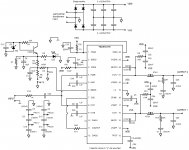
I made a schematic of the initial circuit. It is appended below.
I discovered reasons why this board should not be used “as is” without some modifications and certainly not at output levels approaching 420W.
* A serious flaw is the use of wrong values for the snubber-circuits (R9/C22/C23 and R13/C33/C34) at the two output lines of the TDA8954TH chip. The correct values are 10 Ohm and 220pF while the initial values used on the board are 10 Ohm and 220nF! The use of far too high capacitor values means that the resistors (10 Ohm) are immediately overloaded and burn to open state, with the result that the snubber-circuits are disconnected. Then, the voltage spikes at the output lines of the TDA8954TH chip are not damped at all and may harm the chip, in particular at high output levels. It is mandatory to replace the snubber-circuit components. On my board, one of the capacitors (C22) was even defect as the capacitor body was missing.
* The heatsink is far too small for high output levels. An efficient, low-noise fan will absolutely be needed. At +/-24V supply and with some 2x2W output (when changed to SE stereo configuration), my heatsink got to good 40 degrees (Celsius), with a room-temperature of 18 degrees, before I used a fan. Imagine the temperature with +/-40V supply and several hundred Watts at the output. Use a fan!
* The supply rails decoupling capacitors (6x2200uF/50V) implemented were not the “Nichicon”-type shown in the advertisement but only cheap “ChongX”-types. 6x2200uF is insufficient for high power levels and should be replaced with a reliable type in order to handle the high ripple currents.
* The output filter capacitors are of the ceramic SMD type (“0603” it seems). With +/-40V supply, I doubt that they can stand the ripple current for long. They should be replaced with film type capacitors.
* In order to reduce switching noise on the analog supply terminals of the TDA8954TH chip, the TDA8954 datasheet recommends the use of 10 Ohm resistors in-between the regular power rails and the analog supply pins of the chip. 1 Ohm resistors are used initially and should be replaced with 10 Ohm for better noise suppression.
* For use at 420W, the PCB should be of a reinforced type with particularly wide copper tracks and eventually thicker (than standard) copper foil. It is not a reinforced type but only standard and the tracks are not particularly wide. I would not take that board to 420W at the output. Modified to stereo 2x80W perhaps (+/-36V supply), but not BTL 420W.
* The output filter chokes have a value of 47uH. This leaves a cut-off frequency near 34KHz. Some will argue that it is a bit low. Worse may be if the more than 10A, for achieving 420W in 8 Ohm, may cause the chokes to saturate in part. Without knowing the specs for the cores and chokes, this remains unknown.
* The small metallic cooling-pad on top of the TDA8954TH housing is electrically connected to VSSA (pins 1 and 24). Therefore, the datasheet recommends use of an insulating sheet between this cooling-pad and the heatsink. Such is not used for the initial design. Without such a sheet, it relies on the insulation from anodizing of the heatsink.
I modified my board into stereo SE configuration by swapping the two input lines to one channel and connect the speakers between each of the output terminals and ground. I:
* replaced the initial snubber components with correct values (10 Ohm/220pF/220pF),
* used a slow-running, low-noise fan for the heatsink,
* replaced the six “ChongX” 2200uF/50V power rails capacitors with Nichicon types,
* replaced the ceramic SMD-type output filter capacitors with good film types (470nF),
* replaced the initial 1 Ohm noise reduction resistors with 10 Ohm ones,
* added two 1uF ceramic capacitors in parallel with C20 and C21 for better noise decoupling,
* replaced two signal input capacitors (C30 and C41) with 1uF film types,
* replaced the two other signal input capacitors (C40 and C26 being connected to ground after swap of input lines) with ceramic “0805”, 4.7uF,
* added two 47K resistors between each input terminal and ground,
* removed C42 and R14 that had become without purpose,
* removed the rectifier bridge and wired the board power rails directly to the power input terminals such that external power rails decoupling would be more efficient,
* stabilized the components with “thermal glue”,
* replaced the two 10uF capacitors with better quality ones as they had anyway been taken out of the PCB to give access for the modifications,
* inserted an insulating sheet between the TDA7854TH housing and the heatsink, adding a fine layer of cooling paste on both sides.
With a +/-24V supply, adding two 10000uF external decoupling capacitors, the modified stereo amplifier sounds just great. As it can be expected from an NXP top-line product. No annoying hum or other noise. I do not intend to use the amplifier above +/-36V supply (2x80W in 8 Ohm).
The board is a typical value-for-money product with good intentions but a careless implementation that necessitates some modifications and suggests further improvements. You get a functional TDA8954TH chip mounted on a reasonable PCB without any real (observed) flaws, decent output filter chokes, decent connection terminals, an acceptable heatsink (to be used with a fan), ceramic signal input capacitors (that may be used) and a mute/standby circuit that actually works.
420W output – not with my board!
Schematic: Initial implementation.
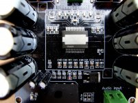
Photo 1: Board before modifications.
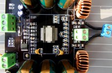
Photo 2: Board after modifications.
Photo 3: Rear side after modifications.
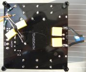
Photo 4: Final board with thermal glue for stabilization.
Photo 5: Rear side with thermal glue for stabilization.
I was tempted by this very cheap (10$) TDA8954TH board (XH-M253) promising 420W (!) mono.
XH M253 TDA8954TH Core BTL Mode HIFI Class 420W High Power Mono Digital Amplifier Board D3 003|Amplifier| - AliExpress
420W I do not need and I find it unlikely in practice but a BTL coupled amplifier, supplied with a symmetrical voltage, can easily be converted into a stereo amplifier with 25% of the power on each channel. It is in principle a matter of swapping the two input lines on one of the channels. However in practice, it may end up more demanding.
I made a schematic of the initial circuit. It is appended below.
I discovered reasons why this board should not be used “as is” without some modifications and certainly not at output levels approaching 420W.
* A serious flaw is the use of wrong values for the snubber-circuits (R9/C22/C23 and R13/C33/C34) at the two output lines of the TDA8954TH chip. The correct values are 10 Ohm and 220pF while the initial values used on the board are 10 Ohm and 220nF! The use of far too high capacitor values means that the resistors (10 Ohm) are immediately overloaded and burn to open state, with the result that the snubber-circuits are disconnected. Then, the voltage spikes at the output lines of the TDA8954TH chip are not damped at all and may harm the chip, in particular at high output levels. It is mandatory to replace the snubber-circuit components. On my board, one of the capacitors (C22) was even defect as the capacitor body was missing.
* The heatsink is far too small for high output levels. An efficient, low-noise fan will absolutely be needed. At +/-24V supply and with some 2x2W output (when changed to SE stereo configuration), my heatsink got to good 40 degrees (Celsius), with a room-temperature of 18 degrees, before I used a fan. Imagine the temperature with +/-40V supply and several hundred Watts at the output. Use a fan!
* The supply rails decoupling capacitors (6x2200uF/50V) implemented were not the “Nichicon”-type shown in the advertisement but only cheap “ChongX”-types. 6x2200uF is insufficient for high power levels and should be replaced with a reliable type in order to handle the high ripple currents.
* The output filter capacitors are of the ceramic SMD type (“0603” it seems). With +/-40V supply, I doubt that they can stand the ripple current for long. They should be replaced with film type capacitors.
* In order to reduce switching noise on the analog supply terminals of the TDA8954TH chip, the TDA8954 datasheet recommends the use of 10 Ohm resistors in-between the regular power rails and the analog supply pins of the chip. 1 Ohm resistors are used initially and should be replaced with 10 Ohm for better noise suppression.
* For use at 420W, the PCB should be of a reinforced type with particularly wide copper tracks and eventually thicker (than standard) copper foil. It is not a reinforced type but only standard and the tracks are not particularly wide. I would not take that board to 420W at the output. Modified to stereo 2x80W perhaps (+/-36V supply), but not BTL 420W.
* The output filter chokes have a value of 47uH. This leaves a cut-off frequency near 34KHz. Some will argue that it is a bit low. Worse may be if the more than 10A, for achieving 420W in 8 Ohm, may cause the chokes to saturate in part. Without knowing the specs for the cores and chokes, this remains unknown.
* The small metallic cooling-pad on top of the TDA8954TH housing is electrically connected to VSSA (pins 1 and 24). Therefore, the datasheet recommends use of an insulating sheet between this cooling-pad and the heatsink. Such is not used for the initial design. Without such a sheet, it relies on the insulation from anodizing of the heatsink.
I modified my board into stereo SE configuration by swapping the two input lines to one channel and connect the speakers between each of the output terminals and ground. I:
* replaced the initial snubber components with correct values (10 Ohm/220pF/220pF),
* used a slow-running, low-noise fan for the heatsink,
* replaced the six “ChongX” 2200uF/50V power rails capacitors with Nichicon types,
* replaced the ceramic SMD-type output filter capacitors with good film types (470nF),
* replaced the initial 1 Ohm noise reduction resistors with 10 Ohm ones,
* added two 1uF ceramic capacitors in parallel with C20 and C21 for better noise decoupling,
* replaced two signal input capacitors (C30 and C41) with 1uF film types,
* replaced the two other signal input capacitors (C40 and C26 being connected to ground after swap of input lines) with ceramic “0805”, 4.7uF,
* added two 47K resistors between each input terminal and ground,
* removed C42 and R14 that had become without purpose,
* removed the rectifier bridge and wired the board power rails directly to the power input terminals such that external power rails decoupling would be more efficient,
* stabilized the components with “thermal glue”,
* replaced the two 10uF capacitors with better quality ones as they had anyway been taken out of the PCB to give access for the modifications,
* inserted an insulating sheet between the TDA7854TH housing and the heatsink, adding a fine layer of cooling paste on both sides.
With a +/-24V supply, adding two 10000uF external decoupling capacitors, the modified stereo amplifier sounds just great. As it can be expected from an NXP top-line product. No annoying hum or other noise. I do not intend to use the amplifier above +/-36V supply (2x80W in 8 Ohm).
The board is a typical value-for-money product with good intentions but a careless implementation that necessitates some modifications and suggests further improvements. You get a functional TDA8954TH chip mounted on a reasonable PCB without any real (observed) flaws, decent output filter chokes, decent connection terminals, an acceptable heatsink (to be used with a fan), ceramic signal input capacitors (that may be used) and a mute/standby circuit that actually works.
420W output – not with my board!
Schematic: Initial implementation.
Photo 1: Board before modifications.
Photo 2: Board after modifications.
Photo 3: Rear side after modifications.
Photo 4: Final board with thermal glue for stabilization.
Photo 5: Rear side with thermal glue for stabilization.
Attachments

Last edited:
Nice posts guys; this should really be a sticky or posted in the Wiki.
There´s just too many people here asking if they should buy this 600W, or rather this 800W SMPS for their "2x225W-amp".
They don´t know that the implementation is unknown or at least sub-optimal and not what is written on the package. That said, most amps will probably do fine at home for a couple of years (if you´re lucky) because most listen to around 1W if even that.
Even a not so good layout can probably put out a couple of watts just fine before it might oscillate.
Heatsink design is difficult with these chips. The pads are small so you´d have to get a big chunk of metal near it to spread. My amp uses thermal paste and a mediating metal plate to connect to a tiny heatsink. So 2xtimes thermal paste which is likely to dry out rather quickly.
2x1W listening level max. would be only 0.4W power disipation (assuming 80% efficiency as above) plus maybe 1-2W quiescent power. That is already up to 2.5W dissipation. Once the thermal paste is dried out the aging of the chip will be pretty fast.
When talking about hundreds of watts one should also consider the DC-connector. as one of many weak links. Some of these are not even rated for 3A permanent.
[OT] Chermann: How do you like that Omnes Audio OBW15PA? I almost bought one but then got a A&D R1524. [OT]
Cheers
Jens
With my experience from posting #12, I checked two other of my TDA8954TH boards for in particular the snubber circuits.
The first and less expensive board is this one:
TDA8954TH Class D High Power Dual Channel Digital Audio Amplifier Board 420W|Circuits| - AliExpress
When I for a start tested this board, I was somewhat disappointed as the high frequencies could appear a bit hard (probably due to distortion). Use of different filter chokes did not really solve the problem. My investigation revealed:
* The snubber components were the same as initially used in posting #12, thus, importantly flawed. The 10 Ohm resistors had burned open.
I replaced the snubber components with the correct 10R/220pF/220pF values.
* No insulating sheet was used between the TDA8954 housing and the heatsink.
With these improvements the amplifier sounded much better, very much like the modified amplifier in posting #12.
The second and more expensive board had already been modified for the protection relay circuit:
HiFi TDA8954TH Dual Channel High Power 2X 210W TDA8954 Stereo Digital Audio Amplifier Board|Circuits| - AliExpress
Check of the snubber circuits showed that both snubber resistors were intact with 10 Ohm. From that I assume that the capacitors have the right value (220pF). No intervention was needed here.
But, no insulating sheet was used between the TDA8954TH housing and the heatsink. The anodizing of the heatsink had in part disappeared where it had contact with the TDA8954TH housing cooling-pad.
I added an insulating sheet.
My conclusion is that if you have a cheap TDA8954 board, check if the subber-circuits are correctly implemented by measuring if the 10 Ohm resistors are intact after use. If the 10 Ohm resistors are intact after use, assume that the capacitor values are correct (220pF).
Wrong snubber components may result in poor sound and eventually damage to the TDA8954 chip.
Last edited:
I was tempted by this very cheap (10$) TDA8954TH board (XH-M253) promising 420W (!) mono.
XH M253 TDA8954TH Core BTL Mode HIFI Class 420W High Power Mono Digital Amplifier Board D3 003|Amplifier| - AliExpress
420W I do not need and I find it unlikely in practice but a BTL coupled amplifier, supplied with a symmetrical voltage, can easily be converted into a stereo amplifier with 25% of the power on each channel. It is in principle a matter of swapping the two input lines on one of the channels. However in practice, it may end up more demanding.
I made a schematic of the initial circuit. It is appended below.
I discovered reasons why this board should not be used “as is” without some modifications and certainly not at output levels approaching 420W.
* A serious flaw is the use of wrong values for the snubber-circuits (R9/C22/C23 and R13/C33/C34) at the two output lines of the TDA8954TH chip. The correct values are 10 Ohm and 220pF while the initial values used on the board are 10 Ohm and 220nF! The use of far too high capacitor values means that the resistors (10 Ohm) are immediately overloaded and burn to open state, with the result that the snubber-circuits are disconnected. Then, the voltage spikes at the output lines of the TDA8954TH chip are not damped at all and may harm the chip, in particular at high output levels. It is mandatory to replace the snubber-circuit components. On my board, one of the capacitors (C22) was even defect as the capacitor body was missing.
* The heatsink is far too small for high output levels. An efficient, low-noise fan will absolutely be needed. At +/-24V supply and with some 2x2W output (when changed to SE stereo configuration), my heatsink got to good 40 degrees (Celsius), with a room-temperature of 18 degrees, before I used a fan. Imagine the temperature with +/-40V supply and several hundred Watts at the output. Use a fan!
* The supply rails decoupling capacitors (6x2200uF/50V) implemented were not the “Nichicon”-type shown in the advertisement but only cheap “ChongX”-types. 6x2200uF is insufficient for high power levels and should be replaced with a reliable type in order to handle the high ripple currents.
* The output filter capacitors are of the ceramic SMD type (“0603” it seems). With +/-40V supply, I doubt that they can stand the ripple current for long. They should be replaced with film type capacitors.
* In order to reduce switching noise on the analog supply terminals of the TDA8954TH chip, the TDA8954 datasheet recommends the use of 10 Ohm resistors in-between the regular power rails and the analog supply pins of the chip. 1 Ohm resistors are used initially and should be replaced with 10 Ohm for better noise suppression.
* For use at 420W, the PCB should be of a reinforced type with particularly wide copper tracks and eventually thicker (than standard) copper foil. It is not a reinforced type but only standard and the tracks are not particularly wide. I would not take that board to 420W at the output. Modified to stereo 2x80W perhaps (+/-36V supply), but not BTL 420W.
* The output filter chokes have a value of 47uH. This leaves a cut-off frequency near 34KHz. Some will argue that it is a bit low. Worse may be if the more than 10A, for achieving 420W in 8 Ohm, may cause the chokes to saturate in part. Without knowing the specs for the cores and chokes, this remains unknown.
* The small metallic cooling-pad on top of the TDA8954TH housing is electrically connected to VSSA (pins 1 and 24). Therefore, the datasheet recommends use of an insulating sheet between this cooling-pad and the heatsink. Such is not used for the initial design. Without such a sheet, it relies on the insulation from anodizing of the heatsink.
I modified my board into stereo SE configuration by swapping the two input lines to one channel and connect the speakers between each of the output terminals and ground. I:
* replaced the initial snubber components with correct values (10 Ohm/220pF/220pF),
* used a slow-running, low-noise fan for the heatsink,
* replaced the six “ChongX” 2200uF/50V power rails capacitors with Nichicon types,
* replaced the ceramic SMD-type output filter capacitors with good film types (470nF),
* replaced the initial 1 Ohm noise reduction resistors with 10 Ohm ones,
* added two 1uF ceramic capacitors in parallel with C20 and C21 for better noise decoupling,
* replaced two signal input capacitors (C30 and C41) with 1uF film types,
* replaced the two other signal input capacitors (C40 and C26 being connected to ground after swap of input lines) with ceramic “0805”, 4.7uF,
* added two 47K resistors between each input terminal and ground,
* removed C42 and R14 that had become without purpose,
* removed the rectifier bridge and wired the board power rails directly to the power input terminals such that external power rails decoupling would be more efficient,
* stabilized the components with “thermal glue”,
* replaced the two 10uF capacitors with better quality ones as they had anyway been taken out of the PCB to give access for the modifications,
* inserted an insulating sheet between the TDA7854TH housing and the heatsink, adding a fine layer of cooling paste on both sides.
With a +/-24V supply, adding two 10000uF external decoupling capacitors, the modified stereo amplifier sounds just great. As it can be expected from an NXP top-line product. No annoying hum or other noise. I do not intend to use the amplifier above +/-36V supply (2x80W in 8 Ohm).
The board is a typical value-for-money product with good intentions but a careless implementation that necessitates some modifications and suggests further improvements. You get a functional TDA8954TH chip mounted on a reasonable PCB without any real (observed) flaws, decent output filter chokes, decent connection terminals, an acceptable heatsink (to be used with a fan), ceramic signal input capacitors (that may be used) and a mute/standby circuit that actually works.
420W output – not with my board!
Schematic: Initial implementation.
Photo 1: Board before modifications.
Photo 2: Board after modifications.
Photo 3: Rear side after modifications.
Photo 4: Final board with thermal glue for stabilization.
Photo 5: Rear side with thermal glue for stabilization.
Do you think it would be a good idea to solder wires in parallel with the power tracks to improve the current caryring capacity?
In principle yes if you want to use it for maximum power. Less copper-track resistance will improve the situation somewhat. But, it is not easy. The rear side is generally one big ground plane so the power tracks are on the top plane. They pass below the TDA8954TH chip.
You need a strong fan to remove in the order of 40W of heat from the chip housing. My general conclusion is rather that it is a low-cost implementation of an amplifier that in theory can deliver 420W but the important compromises used for the board will hardly make it possible, disregarding how much effort you put in. The 420W arrives from the TDA8954TH datasheet and not from real testing of the amplifier.
You need a strong fan to remove in the order of 40W of heat from the chip housing. My general conclusion is rather that it is a low-cost implementation of an amplifier that in theory can deliver 420W but the important compromises used for the board will hardly make it possible, disregarding how much effort you put in. The 420W arrives from the TDA8954TH datasheet and not from real testing of the amplifier.
Last edited:
Subwoofer use.
I'm testing this amp to power one of my tapped horn subs:
TDA8954TH 420W Accessoires Gemakkelijk Installeren Core Subwoofer Mono Kanaals Digitale Audio Audio Stereo High Power Module Versterker Board|Versterker| - AliExpress
Having read almost everything on this chip on this forum, I'm using two 12V 225VA transformers, wired in series to get 24-0-24V DC to power the (sofar) unmodified amp. I only added heatconductive paste between the chip and the heatsink (what a crappy way to fasten it...) and added a heatsink to the small(ish) 8A rectifier.
Comparing it to the output of the 150watt plate amp, which powers the other sub, I may be getting around 200W output into the 4 Ohm sub, maybe a bit less, but it works.
As the amp currently sits on top of the cabinet with the flatscreen TV (very low WAF), it gets hot, close to 50°C, It 'll get hotter once in a closed housing...
I don't want to use a fan, as it will be audible.
Would modifying the board, by moving the capacitors to the bottom, or side, so there is room for a substantually larger heatsink, be worth the time and effort to get the amp to run a bit cooler?
Regards, Jan.
Attachments
Hi Jan,
A bigger heatsink will always improve the situation somewhat. But, it will hardly be enough if you really use the sub hard. I use an ultra low-noise 12cm computer fan (12V DC) which I operate with 6V DC and I hear no fan-hiss unless less than 50cm from the fan.
Forced cooling is much more efficient than passive cooling. I would still consider a fan. I paid around 5$ for my fan.
Hi FF,
I gathered as much.
The sub is connected to the LFE output of my receiver (which is non adjustable and puts out just enough to let the sub keep up with the very efficient front speakers) and is predominantly used for stereo music and TV sound.
When watching a film on DVD the theatre soundtrack makes the sub(s) work harder, and the low frequency sound is more present, something my wife isn't too fond of, when the room is pressurised with explosions and earthquakes...
As a test, I swapped the toroid tranformers for much lighter switching power supplies, delivering 24-0-24 V DC, resulting in less heat and less output, now the tapped horn sub can't keep up with my 240cm long tubular sub.
I bypassed the rectifier and connected the 24V to the plus an minus of the capacitors.
The toroids output is definately the way to go, but I'd like to use a switching powersupply (or two), which should deliver 32V DC.
These prove to be very hard to find, other than having it specially made by the Chinese manufacturer.
I'm currently using a 9 cm 12V fan to vent my audio rack (the warm air tends to hover between devices) running on 6V, suspended in rubber bands, but it's stil audible when it's quiet, so I'll have to go for the 'ultra low noise' ones in future.
Going through your modifications in #12, I wonder which one would be beneficial for my subwoofer use of this chip.
Regards, Jan.
Last edited:
The only switching powersupply providing 32-0-32V DC I can find (at the moment) is the one from Connex:
SMPS240R | Connex Electronic
Slightly more expensive than the Chinese made...
And similar to a 2 x 24V Toroid: 2x 24V ringkerntransformator 225VA
Regards, Jan.
SMPS240R | Connex Electronic
Slightly more expensive than the Chinese made...
And similar to a 2 x 24V Toroid: 2x 24V ringkerntransformator 225VA
Regards, Jan.
Last edited:
- Home
- Amplifiers
- Class D
- TDA8954th btL amplifier