The TDA7293 does amazing as a replacement. This below is the amp module which I replaced with a new pair of boards with the LM3886 chip. All as per the Jaycar and Silicon Chip magazine for heat sinks, fan and PSU. Replaced with a Yamaha power amp in 1998 and again replaced with the system with the TDA7293 chips in it. You are prolly correct about the design issue, but I don't know enough to comment on that. Speakers were Aaron Audio Precision 3 or AP3 on custom stands either side of the deskDesign issue, I'd say. Heatsinking capability wasn't sufficient wrt. supply voltage and load impedance. Optionally you needed to parallel more chips.
Best regards!
https://www.alburyrcmodels.com.au/50-watt-amplifier-module-kit
https://www.manualslib.com/manual/204982/Aaron-Ap-3.html?page=3#manual
I would love to get my hands on what you and Sercan come up with. For the moment, I have mixed news with noise in my system, and it is the TDA723 amp section related. It's in a 'musophile' rather than audiophile setup. Pro laptop via USB to either a Yamaha MG12XU console or a Roland DJ-202 and then into a Roland MX1 that runs the DAW and outputs to the desk and sound system, home or live. No noise issues in this setupIt's a good sounded dirty girl.. I've listened it more than 2 months with different DACs.. However in my setup I could hear a deep (high freq) noise when I close to the tweeters about 10cms.. Then I decided to retire her after 2 months listenning.. Because I am a "noise obsessed" listener !!!🙁
But after weeks it occurred to me that the design needed to be improved. In fact we initially asked for help from Bob Cordell, who was the original designer, but he stated that he had no knowledge of LM317s and TDA series chipamps, so I started to examine the circuit. and I realized that the main source of noise was actually the ccs we were using. I replaced the lm317 based ccs with a current regulated diode and a jfet ccs, and had Sercan measure the results (since I did not have the necessary measurement equipment) and we were amazed to see that the background noise had dropped to 30uV (it was 100uV before). This is a very serious development, but I was disappointed that it did not improve the SNR. We are currently focusing on this issue and I believe that we will soon make progress in the SNR
Noise has been an issue with direct sources, such as when using the 'aux' input directly from my older PC and a no name Bluetooth+Instrument mini mixer. I can tap into the direct amp inputs, bypassing the built-in front end, but then it becomes more susceptible to picking up noise as well as hum. On its own, there is no hiss or hum type noise and none when hooked up to the analog console or the digital mixers with music off and volume turned up
Though I can't quite follow the development work that you guys put in, I am looking forward to some fully sorted boards once available

For CCS in DIFF JFET in CFP the 317/337 REG are simply to noisy!
Try 4mA CCS by using ZTX851 or 2N5210 with LED HLMP6000 as CCS REF voltage, LED biased with approx. 3mA.
Or use low noise J112+Rsourse as CCS...
I tried to get as high SNR / low output noise as possible in simulation TINA.
I used a generic OPA541 as the output AMP, because I had it ready from another project, it will suffice to check here for SNR-OUT noise.
With the TDA7293 we can expect similar or slightly worse results.
SNR can be expected around 100dB@1KHz, hardly anything better with this composite/topology, even though we have a very quiet input DIFF CFP.
SIM THD is very good, because with the CFP+AMP composite we have obtained a high OLG,
which will easily correct the accumulated errors.
But TDA7293 has an average SR and we will not get anything faster out of it, although the input discrete JFET CFP is extremely fast.
Somehow we need to get rid of the TDA7293 internal IPS+VAS (since they dictate the DS parameters)
and drive the 7293 directly to pin11 output DMOS fast Buffer as SLAVE!

LP
Dragan
Try 4mA CCS by using ZTX851 or 2N5210 with LED HLMP6000 as CCS REF voltage, LED biased with approx. 3mA.
Or use low noise J112+Rsourse as CCS...
I tried to get as high SNR / low output noise as possible in simulation TINA.
I used a generic OPA541 as the output AMP, because I had it ready from another project, it will suffice to check here for SNR-OUT noise.
With the TDA7293 we can expect similar or slightly worse results.
SNR can be expected around 100dB@1KHz, hardly anything better with this composite/topology, even though we have a very quiet input DIFF CFP.
SIM THD is very good, because with the CFP+AMP composite we have obtained a high OLG,
which will easily correct the accumulated errors.
But TDA7293 has an average SR and we will not get anything faster out of it, although the input discrete JFET CFP is extremely fast.
Somehow we need to get rid of the TDA7293 internal IPS+VAS (since they dictate the DS parameters)
and drive the 7293 directly to pin11 output DMOS fast Buffer as SLAVE!
LP
Dragan
Last edited:
In fact, what I expected from this project in terms of THD was approximately the values in your simulation (like 0.0005%). However, a level like 0.002%, which is the actual value, is also quite acceptable in my opinion. Anyway, the SR of TDA is low as expected, but when I look at it from a musical perspective, I think levels like 7-8v/us are sufficient. I don't mind this.
I think there were two main problems with this amplifier; the first one was the background noise (even when the inputs were short-circuited, it was at the level of 95-100uv) and more importantly; the SNR ratio was quite low as measured.
It seems that we solved the first problem to a great extent with the JFET-based CCS modification (although not as fantastic as in your simulation, it was about 30uv at the output).
The problem we have now is SNR. I think this is a problematic that seriously affects musicality at low levels. Before the JFET CCS modification, the SNR, which seemed to be around 87-88dB, increased to around 91dB after this mod. However, I think there is still a margin. I will suggest the BJT CCS model in your simulation to Sercan and we will apply it and see the results together. I hope the SNR will increase to 93-94dB.
Thank you for everything.
The TDA7293 is a great chip , it sounds about the same as my discrete mosfet amp.
I have to try a current booster so that 45 volt rails can be used into 4 ohms.
I have to try a current booster so that 45 volt rails can be used into 4 ohms.
The TDA723 class HD implementation that I have, I can see all Jfet opamps on the boardsIf you want really low noise why not just replace the JFETs and CCS with a JFET op amp.
The whole circuit will get cleaner and perform better (and cheaper as well).
Blasted some cobwebs at full volume yesterday, it sounds amazingThe TDA7293 is a great chip , it sounds about the same as my discrete mosfet amp
I peeked inside a long time ago. There are two TDA723 chips, one per channel. There are also quite a few Jfet opamps on the PCB. It's made by a large scale audio modules only for brands builder with a lot of confidentiality statements and requirements to the systems buildersBTW what do you mean by that?
The difference that I hear between this system and a TDA723 module from eBay on a fairly decent PSU might be the differences in the PSU and input section. How can Class HD be used with this chip?
We want to reach an improved vintage-modern sound. There are LM3886 and TDA729X amplifiers made with opamps on the market and we are a bit bored with these applications. We continue to improve the small flaws of this amplifier. Because this class A buffer sounds really good.If you want really low noise why not just replace the JFETs and CCS with a JFET op amp.
The whole circuit will get cleaner and perform better (and cheaper as well).
The problem we have now is SNR. I think this is a problematic that seriously affects musicality at low levels. Before the JFET CCS modification, the SNR, which seemed to be around 87-88dB, increased to around 91dB after this mod. However, I think there is still a margin. I will suggest the BJT CCS model in your simulation to Sercan and we will apply it and see the results together. I hope the SNR will increase to 93-94dB.
Thank you for everything.
Also try to increase the bias in CCS of DIFF JFET in input CFP to 5.5...6mA per branch,
2.7...3.0mA/JFET and same for BJT.
Also the input impedance for TDA7293 should be low (lower thermal resistors noise) but not too low on -IN pin, because then it worsens the THD!
R18 reduce from current 50K-> to value 15K
R14 2K5 now becomes 820R, TOT gain Ao remains around 25dB
R11 can be left 68R
R12 now 1K9 -> to value 2K4 we can now adjust (with R12) impedance at +IN pin, to the ratio and impedance seen by -IN pin,
to have as small OUT DCoffset as possible, which is then corrected by DCservo opamp anyway.
In SIM this way I gain almost 5dB in SNR @1KHz
LP
Dragan
Is a differential input really necessary for you, or did you design such an DIFF input specifically,
or maybe only SE input will be sufficient?
I'm asking because of lower total noise or overall higher SNR
or maybe only SE input will be sufficient?
I'm asking because of lower total noise or overall higher SNR
Hi DXvideo & sercan85
Maybe a bit of a strange question at this point,
have you measured the SlewRate of the output PowerBuffer before?
Leaving the TDA7293 in Slave mode (as per DS), its input is now PIN 11.
This eliminates the influence of the internal "slow" IPS+VAS, leaving only a 1V/V OUT PowerBuffer.
I wonder how fast the output buffer is?
I am attaching a diagram of one such Large Signal measurement with a PSU of at least +/-30...35VDC
and an square wave input signal of +/-15...20Vpeak @10KHz
The signal generator it can be with a relatively slow SR (>20V/us), then we can measure in two channels mode with an oscilloscope
and the differences between the input and output oscilograms response are then compared.
SR_(from below Paint-oscilogram) => 20V in {450nsec - 250nsec} => 20V/200nsec = 100V/usec
An interesting fact in the DS TDA7293 are two statements that indicate a DMOS structure of the output buffer:
-"To overcome these substantial drawbacks, the use of power MOS devices, which are immune from secondary breakdown is highly desirable."
-"Due to the absence of the 2nd breakdown phenomenon, the SOA of the power DMOS transistors is delimitedonly by a maximum dissipation curve dependent on the duration of the applied stimulus."
?L-DMOS? ...Laterals?
🙂
Last edited:
Since I am very excited, I wanted to inform you about some promising developments about the project before Sercan...
First of all; contrary to what is stated in the datasheet, the TDA7293 is definitely working with 10x gain. No signs of oscillation were observed.
Based on this, we reduced the gain of our amplifier by 10x (20dB) and adjusted the CCSs of the buffer according to dear Dragan's suggestion.
The results proved that we made serious improvements;
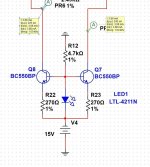
When we modified our circuit with a simple CCS with BC550s and red leds (thanks to Dragan), we achieved 18.5uV noise at outputs while inputs shorted, 0.00093% THD for 8ohm 1w and an incredible 98.5dB SNR.
The JFET pair we used for the buffer was still JFE2140 (we could not get better results with the more expensive LSK489)..
First of all; contrary to what is stated in the datasheet, the TDA7293 is definitely working with 10x gain. No signs of oscillation were observed.
Based on this, we reduced the gain of our amplifier by 10x (20dB) and adjusted the CCSs of the buffer according to dear Dragan's suggestion.
The results proved that we made serious improvements;
When we modified our circuit with a simple CCS with BC550s and red leds (thanks to Dragan), we achieved 18.5uV noise at outputs while inputs shorted, 0.00093% THD for 8ohm 1w and an incredible 98.5dB SNR.
The JFET pair we used for the buffer was still JFE2140 (we could not get better results with the more expensive LSK489)..
Attachments


Under the coordination of @Dxvideo , we conducted multiple measurements using various CCS configurations, including the E-425 diode, 2SK880BL, JFE2140 (CCS), and BJT LED CCS. Interestingly, we achieved noise levels of 28-30 µV at 20x gain and 18-20 µV at 10x gain.
Since matching 2SK880BLs is a tedious process, we had to use trimmers to adjust the branch currents. However, this was a bit too cumbersome for DIY audio builders. The JFE2140, being a matched dual JFET, worked excellently with two 135Ω resistors per branch, but it was unnecessarily expensive for this particular application and didn’t provide a significant advantage.
For the E-425 diode, finding matched pairs within the 4mA–4.20mA range required purchasing at least 20 pieces, and aside from noise performance, it was not particularly successful in our tests. On the other hand, @Dragan100 ‘s CCS performed excellently, providing 4mA per branch. I only performed hFE matching for the BC550C transistors.
For this position, MPSA18 and BC550 could work well, but we concluded that a low-noise, matched dual NPN transistor in an SMD package would be much better. Therefore, in our new PCB design, we decided to use PMP4501Y,135, and we will most likely use MELF204 resistors. The LED will be LTL-4211N.
Surprisingly, the TDA7293 did not oscillate at 10x gain, and—just like the LM3886 miracle—we achieved low THD and low SNR. We will repeat our measurements and introduce several innovations in the new PCB, particularly to improve usability. Specifically, we will design an SOIC-8 footprint that is also DIP-8 compatible, allowing users to experiment with different JFETs.
Please do not hesitate to share your suggestions, we will continue to develop this amplifier together.
Thanks for your support!"
Congrats!!! @sercan85 and @Dxvideo
At 1W RMS / 8Ω, the THD of 0.00093% and SNR of 98.5 dB are excellent results.
In the TDA7293 datasheet, the total input noise (20Hz–20kHz) is specified as typical 3µV to a maximum of 10µV with inputs shorted and a 26dB gain.
With an overall gain of 10V/V, this results in 18.5µV RMS at the output with an 8Ω load.
Thus, we can deduce that the TDA7293 with a 10V/V closed-loop gain in this composite amplifier achieves an SNR margin of approximately 104dB.
There is potential for further SNR improvement.
With 2mA per JFET in a CFP input differential pair, combined with a 2mA-biased low-noise 2N5087, we are optimizing noise performance.
Possible alternative BJTs include:
At 1W RMS / 8Ω, the THD of 0.00093% and SNR of 98.5 dB are excellent results.
In the TDA7293 datasheet, the total input noise (20Hz–20kHz) is specified as typical 3µV to a maximum of 10µV with inputs shorted and a 26dB gain.
With an overall gain of 10V/V, this results in 18.5µV RMS at the output with an 8Ω load.
Thus, we can deduce that the TDA7293 with a 10V/V closed-loop gain in this composite amplifier achieves an SNR margin of approximately 104dB.
There is potential for further SNR improvement.
JFET & BJT Selection
The JFE2140 matched pair is currently the best choice for ultra-low noise JFETs.With 2mA per JFET in a CFP input differential pair, combined with a 2mA-biased low-noise 2N5087, we are optimizing noise performance.
Possible alternative BJTs include:
- ZTX951, ZXTP2027, 2SA2713, 2SA1163, 2SA4117
- If removing the 150Ω degeneration resistor, a matched HN4C06J pair could be used.
Enhancements for the Input Differential CCS
- Use ultra-low noise BJTs, such as ZTX851, ZXTN2018, or a matched Toshiba HN4C51J pair.
- Implement an ultra-low noise voltage reference, such as a HLMP6000 LED biased at 3–3.5mA.
- Alternatively, use a string of 2–3 low-noise 1N4148 diodes, biased at ≥1mA.
Optimizing TDA7293 NFB Impedance
- Lowering the TDA7293 input impedance could help, but lowering to match it completely degrades THD.
- SIM results suggest that a 12kΩ–1.2kΩ NFB combination provides some dB SNR improvements, while keeping 68Ω–2.4kΩ on the +IN pin.
This was the last versions graphics. (4 ma bias, jfe2140+bc550+pn4250 with 49k9/4k7 nfb)

we did your recommendations @Dragan100
First, bias increased to 5.65ma per leg, replaced nfb resistors to = 12k/1k2, and tda's input resistor 1K9 to 2K4. This is the results;
SNR increased appx 1db (may be in measurements uncertainity margin) but thd also increased nearly 5 times.
because of 2.harmonics peak (appx -78dB which is audible I guess)
I will listen amplifier with and without your mods and compare my feelings and will report the result..
Last edited:
Great job!
With this composite configuration—an input DIFF JFET in CFP combined with a TDA7293 PowerOpAmp in local negative feedback (NFB)—we are navigating a trade-off between SNR and THD.
The key factor lies in the impedance loading of the +IN and -IN inputs of the TDA7293.
Lower impedance results in reduced input noise for the TDA, thereby improving the SNR ratio. However, this also places a greater load on the input DIFF stage. To mitigate this, I suggested increasing the DIFF bias, ensuring that it can handle the increased load more effectively, maintaining a higher bias reserve in Class A operation.
For SIM Tina, I used the TI OPA541 macro model as a stand-in for the TDA7293, though it has slightly different characteristics. From my SIM tests, the configurations I previously recommended provided the best balance.
Ultimately, the choice comes down to your preference for THD vs. SNR optimization.
In one of your earlier posts, you mentioned:
The latest SNR and THD measurements confirmed that trend!
SNR improved slightly (though further SNR improvements are unlikely with TDA7293, because of no Global NFB),
while the "tube sound" became more prominent, 🙂
especially with the 2nd and 4th harmonics, showed up more strongly with to low NFB loading—and perhaps slightly too pronounced.
Given this, I suggest some further experimentation.
Trial and error is your best approach at this stage (is all I can recommend at this point)
—you’re definitely close to an optimal balance between minimum THD and maximum SNR.
Here are a few things to try:
Let me know how it goes!
With this composite configuration—an input DIFF JFET in CFP combined with a TDA7293 PowerOpAmp in local negative feedback (NFB)—we are navigating a trade-off between SNR and THD.
The key factor lies in the impedance loading of the +IN and -IN inputs of the TDA7293.
Lower impedance results in reduced input noise for the TDA, thereby improving the SNR ratio. However, this also places a greater load on the input DIFF stage. To mitigate this, I suggested increasing the DIFF bias, ensuring that it can handle the increased load more effectively, maintaining a higher bias reserve in Class A operation.
For SIM Tina, I used the TI OPA541 macro model as a stand-in for the TDA7293, though it has slightly different characteristics. From my SIM tests, the configurations I previously recommended provided the best balance.
Ultimately, the choice comes down to your preference for THD vs. SNR optimization.
In one of your earlier posts, you mentioned:
...might have some tube sound as well....
The latest SNR and THD measurements confirmed that trend!
SNR improved slightly (though further SNR improvements are unlikely with TDA7293, because of no Global NFB),
while the "tube sound" became more prominent, 🙂
especially with the 2nd and 4th harmonics, showed up more strongly with to low NFB loading—and perhaps slightly too pronounced.
Given this, I suggest some further experimentation.
Trial and error is your best approach at this stage (is all I can recommend at this point)
—you’re definitely close to an optimal balance between minimum THD and maximum SNR.
Here are a few things to try:
- Modify the NFB network (currently 12K - 1K2). Test a slightly higher DIFF load, such as 15K - 1K5 in NFB, and observe the effect THD vs SNR.
- you also have to adjust the impedance at the +IN input of the TDA7293 at the same time so that it doesn't get too low and thus load the input DIFF heavely.
- This adjustment is also essential for DCservo, because with a balanced correction of the load on inputs +IN in relation to the load on -IN , the output of the DCservo opamp will be around 0V (+/-1V is OK) {try NFB combination 18K-1K8, +IN 220R-2K7}
Let me know how it goes!
Attachments
I'm really curious about the slew rate (SR) performance of the TDA7293 Output Unity Gain DMOS Power Buffer.I will measure it and let you know.
I already have a clear concept for implementing it with a fast, high open-loop gain (OLG) front end.
Have you had a chance to run these SR measurements yet?
https://www.diyaudio.com/community/attachments/tda7293-sr-measure-jpg.1414933/
Looking forward to the results!
You might be interested in the some your next project
—a variation of the DIFF stage using JFE2140 + TDA7293, now featuring Active Bias (DC + AC) and a DC servo.
With global NFB from OUT to the JFE2140 input, this configuration achieves:
high open-loop gain (OLG), excellent SNR, strong DC performance, and a wide bandwidth...etc
Active bias actually helps to increase the TOT OLG!
Now that the TDA7293 operates in a composite and closed-loop setup,
its input voltage noise and slightly lower SNR effectively become an accumulated error
—one that the input DIFF stage detects and corrects within the total OLG capacity.
Check out the SIM results!
I’ve also attached the Tina simulation file

EDIT:
I forgot to add:
We keep JFETs Uds around 3...4,5V with ActiveBias, so we don't need a Cascode input,
at Id @2.25ma and Uds @3,7V (per JFET) we don't have increased thermals and thus increased thermal noise
—a variation of the DIFF stage using JFE2140 + TDA7293, now featuring Active Bias (DC + AC) and a DC servo.
With global NFB from OUT to the JFE2140 input, this configuration achieves:
high open-loop gain (OLG), excellent SNR, strong DC performance, and a wide bandwidth...etc
Active bias actually helps to increase the TOT OLG!
Now that the TDA7293 operates in a composite and closed-loop setup,
its input voltage noise and slightly lower SNR effectively become an accumulated error
—one that the input DIFF stage detects and corrects within the total OLG capacity.
Check out the SIM results!
I’ve also attached the Tina simulation file
EDIT:
I forgot to add:
We keep JFETs Uds around 3...4,5V with ActiveBias, so we don't need a Cascode input,
at Id @2.25ma and Uds @3,7V (per JFET) we don't have increased thermals and thus increased thermal noise
Attachments
Last edited:
we did your recommendations @Dragan100
bias are 5.65ma per leg, replaced nfb resistors to = 18k/1k5, and tda's input resistor 68 to 220, 1K9 to 2K7. This is the results;
I think Rin and Rin L can stay as the same 68 and 1.9K

bias are 5.65ma per leg, replaced nfb resistors to = 18k/1k5, and tda's input resistor 68 to 220, 1K9 to 2K7. This is the results;
I think Rin and Rin L can stay as the same 68 and 1.9K
Last edited:
- Home
- Amplifiers
- Chip Amps
- TDA7293+JFE2140(LSK489)composite feedback amplifier