In the PCM63 datasheet they say that DAC is -2 to +2 mA. Whats the funktion of bipolar offset current i don´t understand. But i can´t see what would be a very big problem in this current offset. Why shouldn´t the stage work with little different current values?
Till,
Inverting after the DAC is not good. The idea to do it in the DAC is to cancel out any garbage on the powersupply which would be on both outputs. Therefore +L/-L +R/-R is better than +L/+R -L/-R since you have one powerline for +L/-L instead of two (in theory).
The pcm63 has a pin BPO (5) which is a bipolar offset current output pin (+2mA). When connected to 6 (out) you get an output of +/- 2mA. Without it, output on pin 6 will be 0 to -4mA like TDA1541. Kirchhoff is watching:
output full positive:
out + offset = 0 + 2 = 2
output at data 'zero'
out + offset = -2 + 2 = 0
output full negative:
out + offset = -4 + 2 = -2
hope this makes it clear
So when offset is connected like D1 (check the schematics) you get +2/-2 on the i/v circuits. The TDA1541 does not have the +2mA offset pin, so you put 0/-4 on i/v ciruit. Q is can it handle it?
Answer: probably not, otherwise the D1 would not have the offset pin connected (?).
Not inverting the MSB is a bit difficult, since it is in the middle of the dataword. Remember this is 32 bits. One easy solution i see for my DAC: find a spdif receiver which outputs i2s with 16 bit words (dont know if there is one, i'll have a look).
This would but the LSB just before the MSB of the new dataword.
I have WS and WSdelayed. XORing them would give me a signal which is low, except for the time when the LSB is on the dataline!
I can then easily reprogram the GAL to not invert the dataline if (WS XOR WSdelayed) is high. However, the shiftregister i use has to be modified from 32+32 to 16+16. That's a hardware change...
Basic logic would also be possible:
- make a ws delayed like i did
- xor it with ws
- clock the pulse through some shift registers to 'move' it to the
lsb position.
- use that to not invert the dataline at that moment.
Would it be audible
mvg,
The +-2 or 0 to -4 mA problem should be easy to solve in the one or other way.
For inverting the dataword i don´t see why inverting all but the MSB is the right way to the inverted word. If these words are twos complement formated inverting the sign would be inverting the word and then increment by one.
2nd picture in #51:
-2. = B'11110'
INV(11110) = 00001
INC(00001) = 00010
B'00010' = +2.
This made with logic ICs i can´t do. I would need software. Or some kind of logic chip i can program like software.
The device desired looks for me like : serial I2S clock into device, now we have 16Bit words. Invert a copy, inc the copy, clock serial out the noninverted and the inverted with a stable isochrone SCLK at the same phase to two DACs in the format they DAC likes.
Now for the less serios intended part of this posting:
The device could - in case it would be doable what it isn´t - also do the following: Depending on DAC R/L channel muliplexed or to separate lines, and MSB or LSB first, with "quirk" or without, and left or right justified. Idealy this device is also able to real time interpolate a spline thru the words read, and generate words for indermediate timeframes beween the 44100Hz words, and clock them out with n*44100Hz * word. Also it could enhance intermediate words in bitlenght as they are interpolated .... and so on. Good job for a DSP - and 2 Years of development work.
the easiest would be to use a format that isn't 2s complement. One that gives -x from x if you invert all bits from x
But I don't know if this exists.
But I don't know if this exists.
There is not much choice i fear - what we have avaiable is Spdif, and sometimes I2S - out of the transports or CDPs. I would prefer to use the I2S if possible. To tell the CD PRO2 unit - or only those few DSA units out there - to use another format on the I2S than what it sends by default would need the additional task to build a own controller. This task is intersting, but i fear also very time consumtive.
formats:
I 2 S - FS mode (default)
2 I 2 S - 2 FS mode
3 I 2 S - 4 FS mode
4 Sony 16 bit FS
5 Sony 16 bit 2 FS
6 Sony 16 bit 4 FS
7 Sony 18 bit FS
8 Sony 18 bit 2 FS
9 Sony 18 bit 4 FS
81 I 2 S - CD-ROM mode
82 EIAJ CD-ROM mode
I don´t know the format of all these modes, some work to find the specs
formats:
I 2 S - FS mode (default)
2 I 2 S - 2 FS mode
3 I 2 S - 4 FS mode
4 Sony 16 bit FS
5 Sony 16 bit 2 FS
6 Sony 16 bit 4 FS
7 Sony 18 bit FS
8 Sony 18 bit 2 FS
9 Sony 18 bit 4 FS
81 I 2 S - CD-ROM mode
82 EIAJ CD-ROM mode
I don´t know the format of all these modes, some work to find the specs
Let's see if we can easilly invert the SOny format.
If I remember correctly, it's an unsigned format. So for a 16bit data, 32768 means zero
If I remember correctly, it's an unsigned format. So for a 16bit data, 32768 means zero
2nd construction site...
we have to design a controller that at least have to set the DAC mode via DSA and tell the transport to play...
we have to design a controller that at least have to set the DAC mode via DSA and tell the transport to play...
What do you want to do?
To be abble to test many configurations, or simply to set the DAC to a given mode?
If it's the 2nd solution, and that the DAC settings are stored (if they stay the same after a shutdown) you only need a computer
To be abble to test many configurations, or simply to set the DAC to a given mode?
If it's the 2nd solution, and that the DAC settings are stored (if they stay the same after a shutdown) you only need a computer
I don´t think the setting will stay after power down. Do you have a DSA cable, could you try it?
i hope i will be able to describe it in english
A black box, reciveing SPDIF or better I2S.
recieving the words 16Bit for left and right channel MSB first (difficult because of the one bit time offset in I2S, here called the "quirk") and build the inverse. As the word are twos complement this must be done by inverting and increment 1. Than serial transfer this words both syncronous, in inverted and noninverted, to two DACs. One DAC recives inverted and noninverted words for right, the other one for left channel.
In case of TDA1541 DAC this transfer has to be into the DAC in I2S with the "quirk" MSB first, right justified. This means the noninverted and inverted words must be feed time multiplexed like the DAC normally expects right and left channel.
In case we use AD1865, without quirk, with at least 2fs speed, left justified (and 2 zeros added each word for 18Bit). Here the noninverted and inverted are feed into separate lines syncronous, no time multiplexed, as the AD has separate left and right data in. This i think would be an intersteing second step, TDA1541 first because demand should be higher in this board. (?)
please rfbrw and guido, check and correct this.
For me it must be SPDIF because of the Ultracurve which is input & output SPDIF.
So just invert the 16 bit words + add 1 after cs8414 chip ?
How are the words marked in the other signals ?
Start / stop bits ???
So just invert the 16 bit words + add 1 after cs8414 chip ?
How are the words marked in the other signals ?
Start / stop bits ???
No one else is answering so I'll have a go.
I think we are trying to:
get a balanced o/p from TDA1541A or TDA1543N
L- / L+ & R- / R+ to minimise noise
using I2S
without loosing any bits
using logic hardwear with minimum noise & jitter
I think / hope in zero OS mode
I am a digital virgin so I hope my summary is sensible and correct
I hope it won't be too boring for the others if you explain even basic terms / abreviations.
thanks
mike
OK Till you beat me to it !
Bernhard said:Please be human and care for the people who have to go with the crystal receiver chip.
OK, as it happens I have one on order, ( I thought it might come in handy...😉 )
mike
What about using a CS8412 or 14 for your SPDIF and convert to I2S, and at this point the black box device feeding the DACs, this would make it usable also for I2S input from a transport directly by leaving away the reciver. This would fit all.
For the timing http://www.diyaudio.com/forums/showthread.php?postid=341149#post341149
first picture.
description here http://www.diyaudio.com/forums/showthread.php?postid=341183#post341183
we don´t add one bit, we need to invert the words by first step: invert it, second step, increment it by 1. Its still a 16 Bit word now. The 17th bit is truncated --> example inverse of 0. = B'0000000000000000' would be B'1111111111111111' now we inc (B'1111111111111111') and because we truncate result is again 0. = B'0000000000000000') works for all other values also, check http://www.diyaudio.com/forums/showthread.php?postid=341156#post341156 picture 2
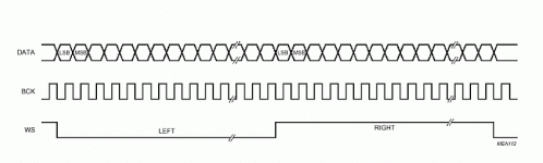
The words are marked by the Wordclock, but to make things not easy god made the word not start at the WCLKs transient but one bit later. Word is bit 2 - 17 of 32 bits, the others are garbage. Bit 2 in one frame of the WCLK is MSB.
I hope this is correct.
For the timing http://www.diyaudio.com/forums/showthread.php?postid=341149#post341149
first picture.
description here http://www.diyaudio.com/forums/showthread.php?postid=341183#post341183
we don´t add one bit, we need to invert the words by first step: invert it, second step, increment it by 1. Its still a 16 Bit word now. The 17th bit is truncated --> example inverse of 0. = B'0000000000000000' would be B'1111111111111111' now we inc (B'1111111111111111') and because we truncate result is again 0. = B'0000000000000000') works for all other values also, check http://www.diyaudio.com/forums/showthread.php?postid=341156#post341156 picture 2
The words are marked by the Wordclock, but to make things not easy god made the word not start at the WCLKs transient but one bit later. Word is bit 2 - 17 of 32 bits, the others are garbage. Bit 2 in one frame of the WCLK is MSB.
I hope this is correct.
till said:What about using a CS8412 or 14 for your SPDIF and convert to I2S, and at this point the black box device feeding the DACs, this would make it usable also for I2S input from a transport directly by leaving away the reciver. This would fit all.
Is that easy to convert to I2S after CS8414 ?
Does your description apply for the standard 3 line signal: SCK SDATA FSYNC ?
Balanced out frpm TDA1541 or TDA1543
Hi,
This has been discussed before:
http://db.audioasylum.com/cgi/m.mpl?forum=tweaks&n=61052&highlight=elso+guido&session=
I stand corrected that the TDA1543A is NOT offset binary but Sony Japanese format.
I fear that the logic scheme needed to correct the LSB for the inverted signal will damage the sound more than leaving the LSB faulty as it is. Also the two DAC's constituting both polarities of the audio signal should be exactly equal. In practice this is not the case.
In case we have a circuit with CS8412 connected to TDA1541 the connection with SCK SDATA FSYNC should be I2S, or? So the CS should be able to give I2S at output
elso,
from TDA1543.pdf:
timing looks exactly like in 1541 datasheet
i don´t really understand your point.
from TDA1543.pdf:
The TDA1543 accepts input serial data formats in two's complement with any bit length. Left and right data words are time multiplexed. The most significant bit (bit 1) must always be first. The format of data input is shown in Fig.5 and Fig.6.
timing looks exactly like in 1541 datasheet
i don´t really understand your point.
Attachments
- Status
- Not open for further replies.
- Home
- Source & Line
- Digital Source
- TDA1541A/S1 Arrangements