Maybe it can be the changed for TDA1540 😀
@diyiggy you know me, I like THT components 😉
>>the Philips SA chip thingy to do it all is bad ?
if I recall correctly, there are some digital filters.
Thanks 🙂
Did You have timings maybe?
Good digging Zoran...not easy to find exactly what you are looking for in his long thread...
Had you studied the sim pcb of your great country fellow Pedja ? Few registers and chip based galvanic async iirc.
What is worryng me, but notice I know nothing about electronic, is all those long traces in term of timing stability and stability in the HF domain... well I know it's not an amp but it is still an electric signal.
Do you need guys some 200 Mhz scopes ? Anyway, that's cool Zoran if your changes are ok...it's hard to definitly say how is sounding a dac chips because it is so much related to all the around design...but I always liked a lot what sounded in my cd player with him and the SAA chip behind.
Hi
I didnt study audial time-sim because it is acomplished with inside xmos settings? So there is no IC chips circuit. And it is for 16bits. Probably it could be posibile to make firmware soft for 14bit? But I dont know really...
.
Yes You have right too long traces are not that good. But also in the BCB we have maybe freater capacitances and other not so good things?
I am using 100MHz scope. (Probes should be better 🙁 anyway is good...
.
I liked the sound of TDA1540 from beguining. And most without oversampling and digital filter SAA 🙁. Even not bad with SAA and OP amps, but somehov slow, muddy, false analog and say politically correct...
.
Somehow I like more TDA1540 then 1541A?
Guys, I need to know why a stopped clock is necessary?
The internal logic in TDA1540 makes sure the clock signal is ignored, and to avoid 'collisons' we could might as well just optimize the timing/synchronisation of the output signals with reference to each other.
Or am I missing something?
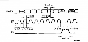
So the 74HC series has a propagation delay of 17 nS for flipflops and 9 nS for standard gates. The HCT series adds 1-2 nS do that.
In the TDA1540 datasheet you can see that the signals needs to be within 10 nS of eachother to be recognised.
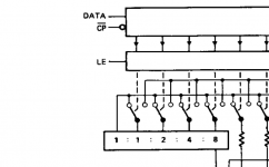
So if we take Miro's circuit in post #1, the data signals are in sync with the output clock signal with the last flipflop's delay only, and the latch signal runs through two gates more than the output clock.
So if we add two inverters in series with the output clock signal, we should have synchronized all the output signals within a few nS.
What are your opinions about the that?
NB: even though I built a functioning version of Miro's circuit, I do not have the equipment to confirm the timings by measurements.
The internal logic in TDA1540 makes sure the clock signal is ignored, and to avoid 'collisons' we could might as well just optimize the timing/synchronisation of the output signals with reference to each other.
Or am I missing something?
So the 74HC series has a propagation delay of 17 nS for flipflops and 9 nS for standard gates. The HCT series adds 1-2 nS do that.
In the TDA1540 datasheet you can see that the signals needs to be within 10 nS of eachother to be recognised.
So if we take Miro's circuit in post #1, the data signals are in sync with the output clock signal with the last flipflop's delay only, and the latch signal runs through two gates more than the output clock.
So if we add two inverters in series with the output clock signal, we should have synchronized all the output signals within a few nS.
What are your opinions about the that?
NB: even though I built a functioning version of Miro's circuit, I do not have the equipment to confirm the timings by measurements.
Attachments
hi
i think that it is not necessery to have stopped BCK. only desireble. Because of less nise injected. And we dont need BCK run all of the time, just when needed?
.
delay information in the datashhets is mostly given at some higher Fo? Byt it is nt the constant and it changes with Fo. As the Fo higher delay we have more delay? So it should be measured for more accurate results?
.
I have digital input slot on the scope that can take up to 16 D inputs and show dierences in timing, maybe i will find the time to build and meassure circuit?
.
Last edited:
Thank you Zoran
I hope you will find the time to build and measure.
I should correct my suggestion to be two unbuffered inverters, or one buffer.
I will maybe try this and see if it actually works at some point soon.
I hope you will find the time to build and measure.
I should correct my suggestion to be two unbuffered inverters, or one buffer.
I will maybe try this and see if it actually works at some point soon.
If You have 2 inputs on the scope maybe You can compare delays with and without? By comparing photos and triggered with same source?
The highest resolution of the X-scale on my 20 MHz scope is 0.2 uS so it will be really tight to see the difference.
20 nS is 1/10 of one square and 2nS will be1/100 of one square.😀
20 nS is 1/10 of one square and 2nS will be1/100 of one square.😀
Hi guys, have you seen this board seeming to have a jumper for both TDA1541 & TDA1540 either ? I2S to simultaneous Converter for TDA1540 DAC or TDA1541 and TDA1541A (no China) | eBay
lin is a courtesy of Icsaszar member in an other thread.
Look at the compact design (short traces) 🙂
however asking myself about the risk of the jumper, I can ear it in my Aya DAC when I'm playing with the different way to input in the tda1541a , soldered straps are way better than jumper or switch here !
Hi guys, have you seen this board seeming to have a jumper for both TDA1541 & TDA1540 either ?
Yes I have seen it.
Very nice.
If Miro´s circuit did not work, I planned to buy that one.
I think it is amazing if you can hear the difference of a jumper vs a soldered connection, but of course I am not going to say anything against it.
But I think with synchronized signals we shold be very close to perfection.
So I measured the timings and added some compensations to get perfect timing, well at least as good as I could get it with my slow scope.
The warm up was reading up on probes and ´building´my own probes trimming the compensation caps to perfect squares.
Also I quickly found out, that ALL the signals ( clock, Latch and 2 x data) benefitted greatly from adding series resistor.
Thanks once again to Zoran for stressing the point of the resistors, and better measuremnet techniques.
So my previuos assumption was, that the two data signals must be delayed as compensation, but actually it turned out, that the clock signal and the latch signal ( who were already in sync with each other) these two needed a small delay to have matching vertical lines with the data signals.
So I took use of the two unused X-OR gates in the 74HCT86, tied one of the inputs in both gates to zero, and let the last input be the /CP and the Latch signal, creating two new /CP and Latch signals with the delay of one gate.
The result is perfect in sync with the data output. ...at least as I can see on my slow scope.
check out the images in the next couple of posts.
Can you elaborate what difference you expect from a soldered vs jumper connection in a digital circuitry?
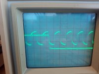
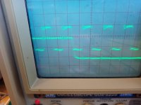
Before compensation.
Picture 1: clock and latch. As you can see already in sync
(Never mind the rounded edges of the clock - it is fixed already in ...)
Picture 2: clock and data.
If you look really close you can see the vertical lines doesn't match.
Picture 1: clock and latch. As you can see already in sync
(Never mind the rounded edges of the clock - it is fixed already in ...)
Picture 2: clock and data.
If you look really close you can see the vertical lines doesn't match.
Attachments
Last edited:
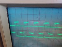
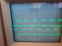
After adding one gate delay to clock and latch.
Tadaaa.
Tadaaa.
Attachments
Last edited:
I am planning to add series resistors to the I2S lines of TDA1541A. What value do you recommend?Also I quickly found out, that ALL the signals ( clock, Latch and 2 x data) benefitted greatly from adding series resistor.
I am planning to add series resistors to the I2S lines of TDA1541A. What value do you recommend?
I use 100 ohms, but the best is to do as Zoran wrote in
post #31 :
"
use 220ohm multiturn small pot. Set to midlle. The goal is to bare in mind informations of recognizing "1" stae value that is lower than +Vb. And "0" that is little before than GND (0) V. This infos are in the PDF for the logic chips. So we dont need any "straight" square and in any case we dont need ringing at the edges. The square should be rounded a bit. Yes the values could be different, from my findings, that is why i suggest to trim. But they are not so different from 68 ohms to 120 ohms. You will see at first time You check it. "
Nrik, it was a surprise ans I performed a test several times...I am not biased here as it was by chance , more exactly it was from a non soldered 1mm copper silver plated vs a vertical jumper soldered with its strap, made from lambda metal tined... yes strange as it is he biasing circuit of the tda 1541 for sim or non simultaneous mode input... strange chip, its grounding is very sensible too and each change can be heard... at least in my system. I noticed that when I changed from the proto board to the definitive setup with the soldered populated parts.
Last edited:
Nrik, it was a surprise ans I performed a test several times...
Amazing.
Anyway: 24bit 48 kHz plays nicely in Miro's circuit as well.
Of course only with 14 bit resolution 😀

- Home
- Source & Line
- Digital Line Level
- TDA1540 - I2S to Offset Binary, no CPLD, no FPGA