Some photos
To follow up on previous post, here's a couple of photos of one board.
Both DC offset and Iq on target but both will drift for quite awhile even with the big heatsink.😡😡


To follow up on previous post, here's a couple of photos of one board.
Both DC offset and Iq on target but both will drift for quite awhile even with the big heatsink.😡😡
Can you define drift - how many mA and what offset are you seeing?
Ideally you just want to drive the amp until the heatsinks settle at their operating temp. 1/3 power get the worst case dissipation situation, but most amps don't work at that level, so I usually say about 50c is ok ( if you have really good heatsinks, then you may not even get to this level)
Then adjust the offset and Iq.
During the process, you may have to tour the current down a bit if it gets excessively high but the objective is just to get to the final operating temp so you can make your adjustment.
I repeat, on my boards the offsett settles at 1-2 mV and the Iq is also stable. Ditto the sx-Amp also.
Iq/Offset profile
Bonsai, here attached is a chart tracking the Iq and DC offset over time, input shorted. With the heat sink I am using, it takes about 45 min for the Iq to settle at around 300 mA as the sink reaches an equilibrium temperature of about 43C. In this test, the offset settles at about 8 mV but can be further adjusted at this point down to +-0V. Seems a long time but without any temperature compensation on the PCB, I guess that can be expected.
Bonsai, here attached is a chart tracking the Iq and DC offset over time, input shorted. With the heat sink I am using, it takes about 45 min for the Iq to settle at around 300 mA as the sink reaches an equilibrium temperature of about 43C. In this test, the offset settles at about 8 mV but can be further adjusted at this point down to +-0V. Seems a long time but without any temperature compensation on the PCB, I guess that can be expected.
Attachments
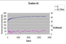
Looks like a drift from +18mVdc when cold to ~ +8mVdc when warm.
That is just 10mV from cold to warm.
That is pretty good.
If you re-adjust down by ~8mVdc, then the cold should be around +10mVdc and the warmed will be in the range +-3mVdc. Those would be excellent figures.
That is just 10mV from cold to warm.
That is pretty good.
If you re-adjust down by ~8mVdc, then the cold should be around +10mVdc and the warmed will be in the range +-3mVdc. Those would be excellent figures.
Yes, they are good numbers. Remember, this is without a servo and the amp is fully DC coupled (just make sure you pre has NO offset - if it does, then capacitively couple it to the nx-Amp. Most pre's are very good in this regard, but you never know).
Nice graph BTW!
How does it sound?
😎
Nice graph BTW!
How does it sound?
😎
I'm close to finishing mine, just been working on rush projects for the DIY day we have in Montreal this coming Sunday. I will give it attention right after.
Ciao!
Do
Ciao!
Do
This is only one channel. As I said, the DC offset can be reset to near 0 once things settle down. I will test the other channel the same way.
Finally got the Speaker Protect on the PSU working. Not sure if it was replacing parts or finally figuring out how to wire it. The build guide it a little difficult when trying to follow all the connects/wires. Really should have a simpler diagram. Anyway, without all the grounding in place etc etc, this channel sounds pretty fine safe for a slight hum/buzz at low volume - but probably grounding related. On to the next channel...
Finally got the Speaker Protect on the PSU working. Not sure if it was replacing parts or finally figuring out how to wire it. The build guide it a little difficult when trying to follow all the connects/wires. Really should have a simpler diagram. Anyway, without all the grounding in place etc etc, this channel sounds pretty fine safe for a slight hum/buzz at low volume - but probably grounding related. On to the next channel...
Finished the second board. Using same parts as first board and matched trannies all in the right places, board behaves like the first for Iq and DC offset, but a difference in voltages at R32/R33! Board I sent pics of had the required 1.0V+-50mV but this second board's value come in at 0.78V +-50mV. Before I start taking things apart, any ideas to explain the difference, to track why or is this another Jim's Audio PCB quirk?
Finished the second board. Using same parts as first board and matched trannies all in the right places, board behaves like the first for Iq and DC offset, but a difference in voltages at R32/R33! Board I sent pics of had the required 1.0V+-50mV but this second board's value come in at 0.78V +-50mV. Before I start taking things apart, any ideas to explain the difference, to track why or is this another Jim's Audio PCB quirk?
You have a first channel working fine so why do you still doubt the Jim's audio pcbs?😕
Fab
Can you suggest an alternative answer as to why I am getting such a difference in the front end with identical and matched components?? I really am not suggesting the boards are at fault but I am a little puzzled. As posted earlier though, I have seen some really bad boards from Jim's. Sooooo...
Can you suggest an alternative answer as to why I am getting such a difference in the front end with identical and matched components?? I really am not suggesting the boards are at fault but I am a little puzzled. As posted earlier though, I have seen some really bad boards from Jim's. Sooooo...
Bonsai is the master of this design so he will sure help you better than I would.
I am just saying that you should be careful before stating that the NX amp pcb from Jim's audio may not be good before you are sure that it is really the case and regardsless of any other experience you may have in the past....
😉
Fab
Last edited:
jprco, if your first amp is working ok and there is an issue on the second amp, I would look for possible misplacement of the resistors - easy mistake to have.
If you are not getting 1V across R32 and R33, then that means you don't have the 1 mA flowing through them that you should have.
Check the voltage across D4 and D3 - should be 10V +- a few 10s of mV
Check that R36 and R37 are correct value - 10k
Check R28 and R29 - must be 15 Ohms
Is J2 shorted?
If you are not getting 1V across R32 and R33, then that means you don't have the 1 mA flowing through them that you should have.
Check the voltage across D4 and D3 - should be 10V +- a few 10s of mV
Check that R36 and R37 are correct value - 10k
Check R28 and R29 - must be 15 Ohms
Is J2 shorted?
Last edited:
Bonsai, thanks for your help.
Every part is in its right place.
Voltage across zeners D3/D4 is 10.5/10.48V on my meter.
I take it you meant R35/R36 should be 15R and they are 15.1/15.1R
R28 and R29 must be 15 Ohms and they are 15.1/15.1R
R34/R35 should be 10K and they are 10.0K/10.01K
R32/R33 should be 1K and they are 1.0K/0.999K
Is J2 shorted? It reads R43 value of 15.1R and input not shorted during measurements.
Voltage across R32/R33: Board No.1 is 1.045/0.993V and although everything above says Board No.2 values should be 1V they are 0.74/0.70V.
I've changed and matched all BC546/556B, BC547/557C and Q6/Q7 several times that now I afraid to damage the PCB. A real poser for me, I may build another board just to see.
Thanks again,
Jean
The 847C pad under my PCB is now ruined from assembly/disassembly. I am thinking of soldering a BC547C in its place. Is that okay and would I have to change anything else?
I am starting to think that this 847C is part of my problem. The pad is very big for such a small SMD and good joints are tough to make.
Jean
I am starting to think that this 847C is part of my problem. The pad is very big for such a small SMD and good joints are tough to make.
Jean
I struggled with that tiny part too. Finally got them working though. This amp is sitting aside waiting for more info once Andrew has built one on these boards. I still don't understand why I had to change R9 to get the offset to work. All seems OK now that I did but I don't understand why yours works with the 10k there and mine wouldn't. Mine sounds a little strident in the upper mids so I'm not sure if there isn't still something amiss. That is why I am waiting before I go any further.
Blessings, Terry
Blessings, Terry
My 2 nd PCB order has left Hzk according to the mail tracker so I should get delivery this week some time.
You do need to use a pair of fine tweezers to put SMD down and a fine tipped soldering iron. Use thin solder as well.
You can change the BC847 for a BC547. The thermal comp won't be quite as good though. I'd really stick with the BC847
You do need to use a pair of fine tweezers to put SMD down and a fine tipped soldering iron. Use thin solder as well.
You can change the BC847 for a BC547. The thermal comp won't be quite as good though. I'd really stick with the BC847
I wish I could stick to the SMD but as I said the pad is kaput! I did manage it on the first board okay. I just want to see if this helps towards resolving my low voltage across R32/33 problem. I did also remove a 1302 as it was shorting to the heat sink. The metal back had a "burr" on it that I missed during install, must have broke through pad on heating. May have contributed to the 847 having to be replaced???
Back to the bench.
Back to the bench.
You can use a single strand of bare copper from a multi-strand cable to connect an SMD component to an adjacent trace.
Pre-tin the trace and both ends of the strand, before trying to solder in place.
Pre-tin the trace and both ends of the strand, before trying to solder in place.
- Home
- Amplifiers
- Solid State
- SX-Amp and NX-Amp