Sadhill
Please can you confirm to me what values you have in your board for
R21
R6 (the pot)
R20
Please can you confirm to me what values you have in your board for
R21
R6 (the pot)
R20
Bonsai,
R6 is 1k (and this is the value I used when I got I=634mA)
R20 is 2.2k (actually 2.19k)
R21 is 1k (actually 0.997k)
I checked Q11, it seems to be ok (without desoldering). 0.33 resistors are ok too (I saw in earlier posts they had to be checked, but that concerned Nx version)
I am now away for a week, so I won't be able to test during that time...
nx amp scaling down
my fault...i saw this very well thought amp design just a couple of days ago.
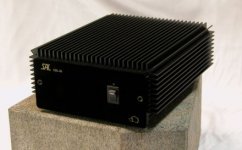
My job is to build an amp that fits into the case see pic... which is very small and serves as the heatsink. My wife loves the design and so...
but due to heatsink size the original amp which gains really moon prices at ebay is rated 40 watts and they used to die on excess temp.
So how to scale the nx down to say +- 28 to 33 Volts does it make sense?
Further there is space for one pair of power BJTs i would use Thermal track NJL4281 / NJL4302 which i think have the same chip as your NJW3281 ....types
my fault...i saw this very well thought amp design just a couple of days ago.
My job is to build an amp that fits into the case see pic... which is very small and serves as the heatsink. My wife loves the design and so...
but due to heatsink size the original amp which gains really moon prices at ebay is rated 40 watts and they used to die on excess temp.
So how to scale the nx down to say +- 28 to 33 Volts does it make sense?
Further there is space for one pair of power BJTs i would use Thermal track NJL4281 / NJL4302 which i think have the same chip as your NJW3281 ....types
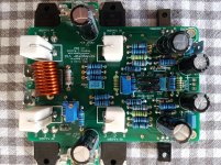
Attachments
On +=28V rails, you will get ~25V peak swing which will give you 40 Watts RMS into 8 Ohms.
One pair of output devices will be fine for 40W RMS output.
You can use the Thermal track NJL devices.
One pair of output devices will be fine for 40W RMS output.
You can use the Thermal track NJL devices.
On +=28V rails, you will get ~25V peak swing which will give you 40 Watts RMS into 8 Ohms.
One pair of output devices will be fine for 40W RMS output.
You can use the Thermal track NJL devices.
yes thanks but the bias current of all stages must be the same as of the original
nx amp? That should be so because of the 10 volts clamp and resistors R30 R31?
so no re-calculation of resistor values required?
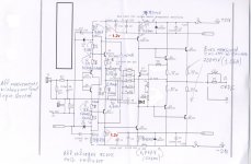
You are correct - you will need to make changes (From V2.10 document V2 PCB).
R18 and R19 - 2.2k (~8.5mA through the 10V zeners). These are 4.7k on the +-50V nx-Amp
re the NJW devices - I have not used these personally, so cannot offer a circuit to use the in built sense diode. My comment above was more to simply say that it is possible to use it.
There are not any other values that will need changing.
I assume you will just use a simple power supply and not the nx-Amp PSU +Protect board?
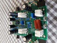
Measuring voltages and checking with the schematic, I think I discovered a bug.
Looks as if the zeners are soldered the wrong way (that is : the way printed on the PCB is wrong...) 🙁
I have to take everything apart to correct it and try again !!!
Hope it did not damage other components...
Looks as if the zeners are soldered the wrong way (that is : the way printed on the PCB is wrong...) 🙁
I have to take everything apart to correct it and try again !!!
Hope it did not damage other components...
It would be easy if you share a picture to determine if zeners are wrongly soldered on your board... you can as well compare with other build pictures posted for SX in the thread to isolate whether zeners are the issue..
No, in fact there is no bug . I did not see D3 and D4 (zeners) were "crossed" between schematic and PCB. Again bad assumption from me...
sorry.
Here are my measurements (with R20 removed as advised), Vpos=Vneg=+/-25V,
I vpos=650mA :
Across R37 : 143mV
Across R36 : 143mV
Zeners 10.3 and -10.3V
Q9 emitter 129mV
Q11 emitter : -156mV
Across R33 : 1.22V
Across R32 : 1.2V
Across R25+R24 : 211mV
Between out and Gnd : 27mV (no way to go lower with R1 adjustment)
Sad hill,
I am traveling now until Wednesday afternoon. I will look at it when I get back. What are your Zener voltages measuring wrt to 0V?
You do seem to have quite a big offset looking at your measurements. Is this problem on both boards?
I am traveling now until Wednesday afternoon. I will look at it when I get back. What are your Zener voltages measuring wrt to 0V?
You do seem to have quite a big offset looking at your measurements. Is this problem on both boards?
Bonsai,
My Zener voltages wrt 0V are more or less the same on the 4 boards : between -10.17 and -10.3V / +10.17 and +10.3V
All boards seem to behave the same : I just blew a DVM fuse again today trying to switch on without lifting R20 on another board.
What about increasing R20 to 4.7k ?
My Zener voltages wrt 0V are more or less the same on the 4 boards : between -10.17 and -10.3V / +10.17 and +10.3V
All boards seem to behave the same : I just blew a DVM fuse again today trying to switch on without lifting R20 on another board.
What about increasing R20 to 4.7k ?
Thimios,
thank you ! It will certainly help but probably later. At present time, as I can't run it without lifting R20 (otherwise very high current in the fuses, blowing either the 6A DVM fuse or the 1A negative rail fuse or both), I'm stuck with unoptimal values...
thank you ! It will certainly help but probably later. At present time, as I can't run it without lifting R20 (otherwise very high current in the fuses, blowing either the 6A DVM fuse or the 1A negative rail fuse or both), I'm stuck with unoptimal values...
- Home
- Amplifiers
- Solid State
- SX-Amp and NX-Amp