That's quite a nice circuit with clear explanation of how each stage works but it is one transistor too many to go on a veroboard.
Oon
That's true too. I remember a circuit with a series resistor at the speaker ground Terminal and another voltage divider at the output of the amplifier. They are then joined by resistors together to create a partial voltage partial current feedback.You can use global feedback to set the damping factor to whatever you want, total control. Feed back (a sample of) the output voltage for low output impedance = high damping factor, or feedback (a sample of) the output current for high output impedance = low damping factor.
Could even use a continuously variable pot to go from low to high damping factor.
Or use a series R at the output of a low output impedance amp ;-)
Jan
The other factor is with simpler circuit without global feedback you will not great distortion figures but the distortion will be lower order and pleasant to the ears.
Oon
That's a pretty smart way of mixing current and voltage feedback.
Oon.
2nd and 3rd order and less of higher order stuff.What do you mean " distortion lower order " with simple circuit with no global feedback?
Oon
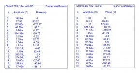
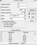
Can you explain what you mean . The first graph is the distortion of post 59 with FB ,the ratio between the 3rd and the 5th is 46.76/0.6=79 on the NO FB it is 308/123=2.5 .

Attachments
Last edited:
2nd and 3rd order and less of higher order stuff.
Oon
This is not a general rule. Sometimes it is, sometimes it is not. The problem is that yopu want to compare nfb with no nfb, all other things being equal.
But that is never the case, there are always other differences as well.
Read Bob Cordell's latest book for when it is, when it is not.
There IS a general rule: with a good feedback amplifier, ALL higher order harmonics are lower than without nfb.
Jan
I am one who considers differential pairs, current mirrors, cascode stages and current sources, as very good building units to design and build a good sounding amplifier. Maybe, I am wrong, but the only pertinent difficulty, that I see to date in employing them, is signals arriving at an inverting input may not have the desired phase and cause oscillations.
How I wish, there was a reliable way of guaranteeing, signals fed into inverting inputs were always in phase with the non-inverting input. The only solution to exist, seems to be using a Miller capacitance, which introduces a 90 degree phase change and rolls gain down with increasing frequency.
How I wish, there was a reliable way of guaranteeing, signals fed into inverting inputs were always in phase with the non-inverting input. The only solution to exist, seems to be using a Miller capacitance, which introduces a 90 degree phase change and rolls gain down with increasing frequency.
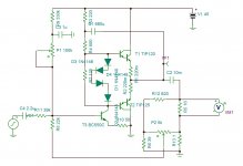
This is class A 3 transistors amplifier 36.6w 8ohms with 0.198% Dtot . A pair of IRFZ44 cost 1$.I don't think the goal is meant to design for 0.2% THD at 10W with 3 transistors.
0.2% for 1W into 8R is more realistic.
Cheers,
Patrick
Attachments
Last edited:
Hi,
Let me see if I figured out some part your circuit. The first transistor serves as a amplifier. The lm317 is a CCS. So a common emitter amplifier with a CCS at the collector results in a huge open loop gain. The 220uf provides a bootstrap that raises the voltage of the bias above positive The output drives the top transistor which is a voltage follower. The bottom part is actually a current sink that is dependent on the input voltage. As the input voltage swings positive the current sink increases the sink as the top part swings low. And you depend on one set or resistors to provide dc + AC feedback. The other is AC feedback. Gain is set very similar to how one sets the gain of an inverting op amp.
How am I doing so far?
Oon
Erase the extension "PDF" of the file bellow and open it in Tina . You can understand and enhance at your wish . You find more explanation of the output stage here .ClassB+a mosfet amplifier.
Attachments
Hi,
I've been thinking on building a class AB amp for my Full range speakers...
Oon
My 2 cents
New amp design ?
http://www.tubecad.com/2008/12/07/power boosters 3.png
http://www.tubecad.com/2011/11/14/Zenlike I-to-V Power Amplifier with PNP.png
http://www.tubecad.com/2009/01/08/inverted diamond buffer topology.png
- Home
- Amplifiers
- Solid State
- Suggestions for simple class AB with no global FB.