the regulation (well actually stabiliser (RJM's x-reg) feeds the whole circuit with power via +/- power planes. the regulation is grounded via the rectification smoothing caps. you could say that the regulation is part of the main circuit to 'smooth out' the DC.
thanks Mark, i'm not up to speed with sims yet but i'm guessing i'm looking at oscillation.
that layout also has the input cold going to the same as the feedback resistor network ground. which would technically put it on the same ground plain. yes? also i dont see an output ground in that layout so sticking a resistor in line to act as a load does not fully represent a speaker.. or am i wrong?
I would say you are wrong on all points.🙂
Local decoupling capacitors must have charging routes that do not impinge on routes for signal. That is much more difficult on the two layer board.
First time I have ever heard of this please enlighten me, as I have never ever seen this done. One ground to rule them all is my motto, the local decouplers are part of the signal loop same ground plane...
thanks Andrew, my main concern now is SGK's thread about these small bridge rectifiers and i'm wondering if they have enough 'juice'. http://www.diyaudio.com/forums/powe...rations-fairchild-sdip-bridge-rectifiers.html
the bridge rectifiers are placed on the underside of the board. i will if needed be making alloy spacers as heat shunts to connect to the base of the case.
well spotted on the volume pot 🙂 thats going to be nippy routing that...
there is no input cold to the opamp, the opamp - is a feedback loop. the resistor going to ground on the feedback is part of the circuit for the feedback to control the gain of the feedback, it has nothing to do with input cold as far as i'm aware. once the hot signal leaves the volume pot it leaves the input cold signal behind, this cold signal as stated before is part of the input from a source and stays part of the source so as not to create trouble in the output signal. the hot signal then goes onto the output amplification which then adds the output cold at the headphone socket. or have i got confusion on this.
yes i really would love a solid ground plain but i really dont know how i'm going to manage to get a full layer pour without opting to use a 3-4 layer board, 3-4 layers is also going to push up the price of boards to get made. to get more layers is going to either cost me money e.g.for a more advanced Eagle editor or find another free editor (pcbexpress?) with the same library as Eagle.
with the amount of traces already on this board a star grounding scheme is out the question. besides why use a star ground when i have a ground plain. i was under the impression that a star grounding scheme only really applies to internal wiring of components to create one fixed ground so not to create a loop.
if i try to reduce the amount of top layer traces to the bottom it's cutting off the negative supply to components. i also thought that having a lot of vias was a bad idea unless you were using smd components to which you can stick them right next to the pad. (note: the design is based very roughly on RJM's Sapphire and if you look at his boards (dual mono) the ground plain is cut up with traces on the top and it manages to sound pretty darn good). from what i can see on my board the biggest problem area for the ground scheme is OPA-1 x-over's causing a restriction.
the board is only 8x10cm and is all through hole components so i think i'm doing well stuffing so much onto one board. if i used smd components then i could place a lot of the components on the underside negating the need for top traces. maybe once i have 'full working' design then yes the use of smd would be superb.
i'm going to give the routing of components a miss for a we while and concentrate on a write up (i'll try and explain what i think each part of the circuit is doing) and BOM then go back to the routing to see if i can organise it a bit better.
my only other option is to go full dual mono with one board stacked on top of the other or side by side but this is going to require either one big transformer or two smaller ones (more AC stray fields floating about), either way its going to make the case real estate bigger and more costly on getting boards made as well as the added cost of the extra transformer. i'm not a rich man.
i really am very grateful for all the help so far and a lot of the suggestions have been very helpful and please keep them coming. its a steep learning curve but fun 🙂
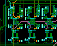
i could not resist having a little play this afternoon...
View attachment 546135
Play about with different placement schemes till you get it right, I generally get analogue with op-amps on single layer routing with maybe the odd trace on another layer... Play with different placements and routing schemes...
If I get time I will look at your design in more detail, trouble is I'm working on site and spend most of the weekend travelling at the moment so time is scarce.
Attachments
H.Ott spends a lot of words/diagrams showing why a two layer PCB does not work properly for implementing planes. H.Ott even shows why 4, 5 and 6 layer boards don't make for perfect plane PCBs.First time I have ever heard of this please enlighten me, as I have never ever seen this done. One ground to rule them all is my motto, the local decouplers are part of the signal loop same ground plane...
I think much of that is down to sharing different current types on the same plane.
Local decoupling injects dirty signals into their common plane. I don't think that common plane should be allowed to contaminate the signal planes.
Local decoupling must be done local to the chip. That requires the local decoupling to be physically very close to the wanted signals. I see that as the difficulty. Keeping the signal routes separated from the decoupling routes.
As I have said previously I never see analogue designs where the local decoupling caps are on a separate ground. Decoupling caps don't inject dirty signals into the ground plane, they provide the near instantaneous power requirements for a device when switching or changing state, they are effectively a very fast local power supply.
You would never do a 5 layer board...
4 layer boards can be a compromise but you can get a contiguous ground plane which is advantageous and there are many 4 layer boards out there that work, as well as many 6 layer boards...
Again for simple analogue designs a single ground is best (with some caveats, mentioned earlier) there is no separate decoupling route or ground they are all connected and to add one is going to cause more issues than a simple plain ground plane...
Marce, this is the way I see it and please correct me if I am wrong. Its the supply and recharging of the decoupling caps that produces the HF currents through the ground plane. After the initial current demand the current reverses direction through the cap. This current is supplied by the next closest capacitor. The solution doesn't have to be a separate layer. Just don't place the audio signal between the power supply and the decoupling caps.
I agree, there are non audio waveform currents passing into and out of the local supply rail decoupling capacitors.Marce, this is the way I see it and please correct me if I am wrong. Its the supply and recharging of the decoupling caps that produces the HF currents through the ground plane. After the initial current demand the current reverses direction through the cap. This current is supplied by the next closest capacitor. The solution doesn't have to be a separate layer. Just don't place the audio signal between the power supply and the decoupling caps.
The route that these dirty currents follow should not contaminate the wanted signal routes.
Just about to drive home from Poole so a quick reply...
The best solution is still a contiguous ground plane... Staring off the local decoupleing caps GND back to the main power supply makes the local decouplers totally useless. If you use a ground plane with routed power lines (often done for analogue designs (they can be seen on the pic I posted yesterday then the pulses will track the power routes to an extent. The other method for really sensitive analogue signals is to route them as a balanced pair (route the signals return path as a broadside coupled pair on adjacent layers). In the majority of cases though the effect will be negligible and on 99% of analogue boards I have seen and worked on a standard ground plane is employed with no problems, it is always best to keep it simple otherwise you can create more problems than you solve.
As said I have had a look at both designs I have done and designs other have done and all have a contiguous ground plane for low level analogue (including headphone circuits).
I have access to about 4000+ designs in our repository many off them analogue...
Now its the M3, A34, M40, M42, M6 on a bank holiday Friday for me.........
You must think in terms of loops, and opamps are NOT 3 terminal devices.
Consider a jellybean opamp with a class AB output stage, now if it is driving a load, what does the loop look like? Starting at the output pin, it goes to the load then to ground, then from the ground return it must get back to one or the other of the power pins, which one depends on which quadrant the opamp is driving into, it is at this point that the decoupling caps come into play, as they provide the local (equals small loop area) path from the ground plane to the appropriate rail.
If you connect the caps to a separate net then you are forcing the current to loop via the junction between the two nets, which is not a good thing as the supply current part of that loop clearly contains extensive harmonics as it is effectively half wave rectified current pulses.
With very few exceptions (The junction of a FWB rectified supply might be one) a solid plane works far better in most cases then trying to second guess where the loops are (Inductive effects usually dominate above a few KHz, the current will tend to flow to minimise loop area even without you doing anything explicit), one good trick is to actually get careful about where you pin down whatever the opamp stage is using as a reference, the junction of the previous stages decoupling caps being a good bet, but a solid plane with good local decoupling and stop worrying will get you 90+% of the way there.
Regards, Dan.
I don't think anyone would disagree with that. The problem is when you (randomly) place the signal components like feedback, input, output and zobel on that same ground plane.
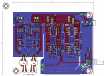
i could not resits tinkering as i had an idea... i have now coupled the input ground plain to the main ground plain via the feedback bias resistors R3-R/L ground pin.
added a lot of vias to clean up the top layer (ground).
now i have a little confusion about the placement of the volume pot. i have placed it after the input coupling capacitors that also act as high pass filters, now i dont know if i have got this right but would this not then act as a variable high pass filter or is having the resistors before cancelling that effect out?
top layer

bottom layer

full layers

added a lot of vias to clean up the top layer (ground).
now i have a little confusion about the placement of the volume pot. i have placed it after the input coupling capacitors that also act as high pass filters, now i dont know if i have got this right but would this not then act as a variable high pass filter or is having the resistors before cancelling that effect out?
top layer
bottom layer
full layers
done a bit of tinkering last night and today with a few headphone amp boards i have. the boards have the input cold on a separate plain and also have a direct connection to COM (main ground plain). on both boards i removed the cold connection from the input cold plain and moved them to the COM. in both instances there was no (listenable) difference, well in fact thats not quite right, i use an RPi as my source which is a nightmare for grounding as it seems that that either the hot or cold output signal does not engage until you start playing a file and up until then there is a very pronounced 50Hz hum. if the RPi and the cold input are left on the separate input ground plain the hum persists when the RPi is turned off and plug removed from mains. with the cold input connected direct to the main ground plain the hum is removed when the RPI is turned off and the plug removed.
either way the hum is not there when the RPi is playing some music on both ways of grounding, its only when the source (RPi) is unplugged from the mains that the connection to COM has no affect on hum.
now here is the right pain, the headphone separate cold input plains are connected to the main ground layer (COM) but via resistor legs of the feedback bias resistor.
what is the above telling me.. that the separate input cold ground plain is causing a loop so the input cold needs to be part of the main ground plain and my original idea of separating the ground plain into sections is a bad idea.
what has come to light is that the COM connection to the main ground plain was also incorrect. add to that the whole power section was a mess.
i also done a bit of searching on the net and in almost all circumstances of a schematic for a non-inverted opamp headphone amplifier (CMoy) everything is connected to a 'virtual' ground. all i'm doing is adding a split power supply with a dedicated COM/GND. then putting 'add on's' to the circuit in the form of a buffer (with by-passing capacitors), and a jfet cascode which can be taken in and out of the circuit if desired which puts the circuit back into the basic CMoy design.
WOW, thanks Mark, that really is going above and beyond the call of duty. its surprised me just how different things can look.
Here's a link to the article that changed my perspective.
The G word: How to get your audio off the ground | EDN
Best regards.
The G word: How to get your audio off the ground | EDN
Best regards.
Here's a link to the article that changed my perspective.
The G word: How to get your audio off the ground | EDN
Best regards.

i have been giving the design less attention at the moment to give my noggin a rest. lol
i have come to the conclusion that 4 layers are going to be the way to go.
using the 4 layers also allows me to remove some of the bugbear traces that i had which has led to all the traces now on the top layer.
going over the data sheets and components i have found a few inconsistency's regarding the pinout, pad placement and sizes on a few components, mainly pots and jacks. this has forced me to learn how to make/change components in library's. all good as its taught me something else.
4 layers.
what will you put on each layer?
Power plane?
Power zero volts/ground plane?
Signal ground plane?
Signal plane?
That puts two planes between signal and power.
What other arrangements are there for a 4 layer board?
what will you put on each layer?
Power plane?
Power zero volts/ground plane?
Signal ground plane?
Signal plane?
That puts two planes between signal and power.
What other arrangements are there for a 4 layer board?
- Status
- Not open for further replies.
- Home
- Amplifiers
- Headphone Systems
- splitting ground planes