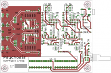
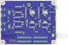
will the GND (COM) layer share both signal returns and power returns?
The link in #96 is an excellent read...
well after some messing around i think i have found a nifty solution, i dont know if it will interfere with the audio signal traces but here goes.
i created a GNDV plane for the DC+/- on the top 'signal' layer. this leaves layer2 for audio GND. the GNDV will be tied to the GND using a via at the input rectification capacitors.
i tried it the other way round but the traces were blocking the path for audio signal GND to create a complete pour.
i created a GNDV plane for the DC+/- on the top 'signal' layer. this leaves layer2 for audio GND. the GNDV will be tied to the GND using a via at the input rectification capacitors.
i tried it the other way round but the traces were blocking the path for audio signal GND to create a complete pour.
had to mess about a bit due to not being able to join the GNDV and GND planes so i made them both GND and manually restricted what was necessary.
i now have:
L1 = signal traces and DC GND plain, the DC GND is connected to the rectification capacitors (COM).
L2 = signal GND plain and is connected to rectification capacitors (COM).
L3 = V- power plain.
L4 = V+ power plain and a few traces that i could not fit on the L1
i now have:
L1 = signal traces and DC GND plain, the DC GND is connected to the rectification capacitors (COM).
L2 = signal GND plain and is connected to rectification capacitors (COM).
L3 = V- power plain.
L4 = V+ power plain and a few traces that i could not fit on the L1
"Star grounding" is never used in modern wide band electronic instrumentation. Bypass capacitors
must return directly to a ground plane, with short leads (if not smt) and short traces, to be effective.
Otherwise, they can even make things worse.
You must think in terms of loops, and opamps are NOT 3 terminal devices.
Consider a jellybean opamp with a class AB output stage, now if it is driving a load, what does the loop look like? Starting at the output pin, it goes to the load then to ground, then from the ground return it must get back to one or the other of the power pins, which one depends on which quadrant the opamp is driving into, it is at this point that the decoupling caps come into play, as they provide the local (equals small loop area) path from the ground plane to the appropriate rail.
If you connect the caps to a separate net then you are forcing the current to loop via the junction between the two nets, which is not a good thing as the supply current part of that loop clearly contains extensive harmonics as it is effectively half wave rectified current pulses.
With very few exceptions (The junction of a FWB rectified supply might be one) a solid plane works far better in most cases then trying to second guess where the loops are (Inductive effects usually dominate above a few KHz, the current will tend to flow to minimise loop area even without you doing anything explicit), one good trick is to actually get careful about where you pin down whatever the opamp stage is using as a reference, the junction of the previous stages decoupling caps being a good bet, but a solid plane with good local decoupling and stop worrying will get you 90+% of the way there.
Regards, Dan.
From the linked article...
How to get your audio off the ground
Bruno Putzeys -April 22, 2014
This article originally appeared in Linear Audio, a book-format audio magazine published half-yearly by Jan Didden.
The G word: How to get your audio off the ground | EDN
The final nail in the star's coffin is that it only works at DC. A wire has inductance and two wires have mutual inductance on top of that. Accidentally lay a "dirty" return wire next to a "clean" reference wire and bam, noise. How do we add power supply decoupling? Do we run long wires from the decoupling capacitor to the star and add exactly as much inductance as we were hoping to get rid of (figure 4)?
Firstly connecting directly at the caps is not recommended, there needs to be some separation of the charging pulses loops from the main GND.
Secondly I presume you are proposing to have the decoupling capacitors on one ground GNDV and the signals on another, this forces the decoupling caps to work through a large loop area, not a good idea as the links I have quoted show, the star will add a high impedance loop... Just a thought.
so if i have the gist of this what i need to do is create a 'busbar' between the +/- of the rectification caps then connect this to the main GND. remove the GNDV and just let one GND rule them all.
i have tried searching the internet for answers but in every instance that i can find they are talking about how to deal with analogue and digital signals and their grounds and power being a separate entity (off board).
i think the penny has just dropped.. make the power section a separate entity with its own ground as if it were off board then connect the audio section ground to that.
If my reading of H.Ott is correct, then the better way to achieve that is to have a signal ground plane next to the signal plane and a separate power ground plane next to the power plane/s...............i think the penny has just dropped.. make the power section a separate entity with its own ground as if it were off board then connect the audio section ground to that.
That gets you to 4 layers as your minimum.
The signal plane is separated from the power plane by two ground planes and these get interconnected at some appropriate location.
Are you saying have the decoupling caps on a separate layer... Don't understand how this would work and why, I think there is (as Brunos document and many others) to much messing around with grounds and ground planes, and it is only on this and other audio based sites that I see grounds played with so much... For a lowish power headphone system I would have one ground plane...
Yes, since the currents passing through the decoupling is not audio. They are effectively dirty currents and contaminate the quality of the voltage on the power ground plane.Are you saying have the decoupling caps on a separate layer
There is likely to be a way to combine the power ground and signal ground planes into a single plane for simpler layouts.... Don't understand how this would work and why, I think there is (as Brunos document and many others) to much messing around with grounds and ground planes, and it is only on this and other audio based sites that I see grounds played with so much... For a lowish power headphone system I would have one ground plane...
But I don't have the skill to even try guiding one to that solution.
I avoid the design complexity of incorporating planes into audio frequency circuits by using discrete traces and not using any planes.
Last edited:
Read the Bruno link earlier, having your decouplers on a separate ground is WRONG, you are adding a huge round trip for the return, as I emphasized by quoting all the replies that said this is wrong....
Posts 106 and 107... All have quotes directly relating to this, i.e. decouplers being on the SAME ground plane to MIMIMISE decouplers loop area
This advice is not correct, by having the decoupling caps on a separate plain or trace you are effectively cutting them out of the circuit may as well leave them of the board, I know of no recommendations to do this other than here and would say it is very bad advice......
This advice is not correct, by having the decoupling caps on a separate plain or trace you are effectively cutting them out of the circuit may as well leave them of the board, I know of no recommendations to do this other than here and would say it is very bad advice......
But if you are taking the decoupling capacitors back to some star point again it is pointless... and again wrong. Having long inductive leads/traces on decoupling caps renders them useless.
There is nothing wrong with ground planes or with the wealth of information out there, it is the sill spiders legs star routing that is wrong, I only see it here on DIY jobs no where else where there is analogue, most if not all the designs I see use ground planes, as pointed out by many we also need to cater for high frequency noise as well as the audio spectrum. As said all analogue designs I see use a ground plane (No I don't see or do many 2 sided boards, most are 4 layers again so they can have a ground plane).
There is nothing wrong with ground planes or with the wealth of information out there, it is the sill spiders legs star routing that is wrong, I only see it here on DIY jobs no where else where there is analogue, most if not all the designs I see use ground planes, as pointed out by many we also need to cater for high frequency noise as well as the audio spectrum. As said all analogue designs I see use a ground plane (No I don't see or do many 2 sided boards, most are 4 layers again so they can have a ground plane).
I don't advocate star grounding for audio current connections. It increases loop area.
All inter-module connections must be done with close coupled flow and return pairs.
The same applies on a PCB, the flow and return pairs must be close coupled.
For decoupling where the non audio currents can be at very high frequency, there must be short loops, that minmise inductance.
I can design for discrete traces. I can see where the current loops should be and incorporate that into component layout.
this is what i'm thinking about now for grounds.
L1, this is the top layer with the power section, the power section has its own ground plane which connects to L2 via the COM through hole.

L2 is the main ground for decoupling caps and audio signal which is connected to the power section ground via the COM through hole.

the other two layers will be for the DC +/- power planes.
L1, this is the top layer with the power section, the power section has its own ground plane which connects to L2 via the COM through hole.

L2 is the main ground for decoupling caps and audio signal which is connected to the power section ground via the COM through hole.

the other two layers will be for the DC +/- power planes.
I don't advocate star grounding for audio current connections. It increases loop area.
All inter-module connections must be done with close coupled flow and return pairs.
The same applies on a PCB, the flow and return pairs must be close coupled.
For decoupling where the non audio currents can be at very high frequency, there must be short loops, that minmise inductance.
I can design for discrete traces. I can see where the current loops should be and incorporate that into component layout.
Yes I can see you view and many years ago two layer designs were done this way, mainly digital funnily enough, though these days ground planes are preferred to help tame any HF interference that a circuit may encounter and to provide a better return path....
my preferred method for low level analogue signals is balanced (or differential) routing an option that I have mentioned many times...
Bibio, on first look I think that will be OK but I will try and look in more detail.
the power section has its own ground plane which connects to L2 via the COM through hole.
Why ?😕 The place where they join should be the output of your regulators. Which means the ground pins of the caps at the output of your regulators, btw. Which caps seem oddly missing ?
The groundplane in L1 and L2 should barely overlap if you lay out things properly.
i'm not using regulators in the normal sense. i'm using RJM's X-Reg. the X-Reg uses NPN/PNP transistors as its output for the +/- voltages so no caps after that unless smoothing caps. to feed the X-Reg i'm using split supply from bridge rectifiers which are connected to smoothing caps, these smoothing caps create the ground via their alternate +/- like creating a virtual ground on battery's. the smoothed voltage is then fed to the X-Reg circuit.
- Status
- Not open for further replies.
- Home
- Amplifiers
- Headphone Systems
- splitting ground planes