thanks syr, interesting idea but i fear that i have way too many traces on the board for doing that. i have a lot of ground points to take care of due to capacitor bypassing and such.
i have a lot of ground points to take care of due to capacitor bypassing and such.
"Star grounding" is never used in modern wide band electronic instrumentation. Bypass capacitors
must return directly to a ground plane, with short leads (if not smt) and short traces, to be effective.
Otherwise, they can even make things worse.
Last edited:
Just use planes with Syr's layout. Input Ground plane, Ground "star" plane and PS-Gr plane. It also shows where the different components and signals should be connected. Feedback to input. Output and PS-Gr to Ground star.
The only thing I would do differently is split the input ground into two (one for each channel) and use a 1-3R resistor per channel.
The only thing I would do differently is split the input ground into two (one for each channel) and use a 1-3R resistor per channel.
Last edited:
here goes again.. lol
Full Board,


Audio Section,


Power Section,


Eagle Files,
View attachment Psychosis Eagle Files.zip
Full Board,
Audio Section,
Power Section,
Eagle Files,
View attachment Psychosis Eagle Files.zip
Yes, sure. But .... we are talking about BUF634 and OPA134, and they are not that modern."Star grounding" is never used in modern wide band electronic instrumentation. .
@Bibio:
I wonder what advantages you hope to gain by using double-sided plates. Your circuit is much simpler and doesn't need them. However, as I said, I had already built it some time ago, but I wasn't too pleased with the sound. I'd recommend that you read this link. This circuit is entirely discrete and, in my opinion, it sounds better. I could attach some pics, should you be interested.
here goes again.. lol
You're getting the hang of it. Look around for the various places where you can move a trace
to the other side of the board, and then fill in the gap in the plane that remains.
Hi syr, the two power planes are easier than trying to route traces, its already very crowded in there.
the amp is based roughly on RJM's Sapphire which sounds superb but he uses a discrete buffer.
the whole idea of this amp is for testing/learning purposes. this is why i have included jumpers so i can take things in and out of the circuit like the Jfet cascode and the buf364 out i just need to jumper across, doing this will give me a basic cmoy amp as a base. a lot of the resistors will also be placed on jumpers.
when i assemble the board i will be placing all the capacitors above the hight of the opamp in the audio side under the board, this is so i can build discrete buffers that will plug in to the DIP-8 sockets. the buffers will be tested off board first by using vero board with the relevant points plugged into the opamp sockets, once i'm happy then i'll get daughter boards made up.
the amp is more of a 'base' design than a fully working amp.
You're getting the hang of it. Look around for the various places where you can move a trace
to the other side of the board, and then fill in the gap in the plane that remains.
i have been trying... lol
i have been trying... lol
It's best to set things aside for a day or two, and then look it over freshly.
Bibio,
your smoothing capacitor charging circuit is good.
You have pairs of traces from transformer ~~ to the rectifier and then pairs of traces to the capacitors.
You have a single connection for Zero Volts.
That whole section works properly with fairly low interference. The only improvement that may give no measureable difference is to move the pairs of traces closer together to reduce the LOOP AREAS.
The amp part needs a lot of work still. Perhaps it is better to explain why A should be connected to B and not to C.
In an ideal layout the +input and the -input of the op-amp would be reverenced to a single point with both the input and output returns (grounds) also connected to this point (star GND).
When we separate the +input reverence point and the input return from the -input reverence point, currents between these two points, created by ground loops or capacitor charging, will cause an error voltage between the op-amp +/-inputs.
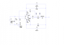
I think that the pot is incorrectly connected. Normally you would connect the source to 1+3 and pin 2 to the amp.
In an ideal layout the +input and the -input of the op-amp would be reverenced to a single point with both the input and output returns (grounds) also connected to this point (star GND).
When we separate the +input reverence point and the input return from the -input reverence point, currents between these two points, created by ground loops or capacitor charging, will cause an error voltage between the op-amp +/-inputs.
I think that the pot is incorrectly connected. Normally you would connect the source to 1+3 and pin 2 to the amp.
Last edited:
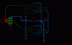
At the moment as others have said you don't have a ground plane but random areas of copper pours... Not a good idea, unless you have a contiguous ground plane to connect these pours too with stitching via's...
Look at placement and try and get all the routes on the top layer and then use the bottom layer as the ground, with minimal slots and gaps, possibly use oblong pads on devices to allow copper pours between pads.
As Rayma has said the caps charging pulses should be a separate ground with a single point connection to the main ground, making sure this point is outside of the AC charging loop (tis is what a starpoint is, not silly skinny spiders legs tracks).
Another point to remember with AC loops is the wavefront moves down the hot and return path at the same time, it is not like a train and carriages going round in a circle as this illustrates..... as well as other good information...
http://www.x2y.com/filters/TechDay0...log_Designs_Demand_GoodPCBLayouts _JohnWu.pdf
Last edited:
The AC charging of the smoothing capacitors is separate. See my post71 and how it refers to post65.
The charging route across the link between the +ve and -ve side of the Zero Volts line has ONE connection to the adjacent plane.
The smoothing cap charging pulses do not pass through that plane.
Local decoupling capacitors must have charging routes that do not impinge on routes for signal. That is much more difficult on the two layer board.
thanks Andrew, my main concern now is SGK's thread about these small bridge rectifiers and i'm wondering if they have enough 'juice'. http://www.diyaudio.com/forums/powe...rations-fairchild-sdip-bridge-rectifiers.html
the bridge rectifiers are placed on the underside of the board. i will if needed be making alloy spacers as heat shunts to connect to the base of the case.
well spotted on the volume pot 🙂 thats going to be nippy routing that...
there is no input cold to the opamp, the opamp - is a feedback loop. the resistor going to ground on the feedback is part of the circuit for the feedback to control the gain of the feedback, it has nothing to do with input cold as far as i'm aware. once the hot signal leaves the volume pot it leaves the input cold signal behind, this cold signal as stated before is part of the input from a source and stays part of the source so as not to create trouble in the output signal. the hot signal then goes onto the output amplification which then adds the output cold at the headphone socket. or have i got confusion on this.
yes i really would love a solid ground plain but i really dont know how i'm going to manage to get a full layer pour without opting to use a 3-4 layer board, 3-4 layers is also going to push up the price of boards to get made. to get more layers is going to either cost me money e.g.for a more advanced Eagle editor or find another free editor (pcbexpress?) with the same library as Eagle.
with the amount of traces already on this board a star grounding scheme is out the question. besides why use a star ground when i have a ground plain. i was under the impression that a star grounding scheme only really applies to internal wiring of components to create one fixed ground so not to create a loop.
if i try to reduce the amount of top layer traces to the bottom it's cutting off the negative supply to components. i also thought that having a lot of vias was a bad idea unless you were using smd components to which you can stick them right next to the pad. (note: the design is based very roughly on RJM's Sapphire and if you look at his boards (dual mono) the ground plain is cut up with traces on the top and it manages to sound pretty darn good). from what i can see on my board the biggest problem area for the ground scheme is OPA-1 x-over's causing a restriction.
the board is only 8x10cm and is all through hole components so i think i'm doing well stuffing so much onto one board. if i used smd components then i could place a lot of the components on the underside negating the need for top traces. maybe once i have 'full working' design then yes the use of smd would be superb.
i'm going to give the routing of components a miss for a we while and concentrate on a write up (i'll try and explain what i think each part of the circuit is doing) and BOM then go back to the routing to see if i can organise it a bit better.
my only other option is to go full dual mono with one board stacked on top of the other or side by side but this is going to require either one big transformer or two smaller ones (more AC stray fields floating about), either way its going to make the case real estate bigger and more costly on getting boards made as well as the added cost of the extra transformer. i'm not a rich man.
i really am very grateful for all the help so far and a lot of the suggestions have been very helpful and please keep them coming. its a steep learning curve but fun 🙂
i could not resist having a little play this afternoon...
thanks Mark, i'm not up to speed with sims yet but i'm guessing i'm looking at oscillation.
that layout also has the input cold going to the same as the feedback resistor network ground. which would technically put it on the same ground plain. yes? also i dont see an output ground in that layout so sticking a resistor in line to act as a load does not fully represent a speaker.. or am i wrong?
that layout also has the input cold going to the same as the feedback resistor network ground. which would technically put it on the same ground plain. yes? also i dont see an output ground in that layout so sticking a resistor in line to act as a load does not fully represent a speaker.. or am i wrong?
i dont see an output ground in that layout so sticking a resistor in line to act as a load
does not fully represent a speaker.. or am i wrong?
The speaker common should return to a stub off the common connection of the main filter capacitors
in the power supply. That's where the output current came from, through the output devices.
Simulations often don't take all of the parasitics into account.
Last edited:
The speaker common should return to a stub off the common connection of the main filter capacitors
in the power supply. That's where the output current came from, through the output devices.
Simulations often don't take all of the parasitics into account.
the headphone socket (output cold) is in a way its just going via the ground plain. i take it that a separate trace to the stub would be better? if is then its going to be going into the 'noisy' rec/reg area to do so.
i could have my wires crossed but i think Mark was on about my hot/cold input scheme being wrong.
the headphone socket (output cold) is in a way its just going via the ground plain.
i take it that a separate trace to the stub would be better? if is then its going to be
going into the 'noisy' rec/reg area to do so.
Does the regulator power the output stage directly? If so, then the speaker common
should go to a carefully chosen place in the regulator's ground plane.
- Status
- Not open for further replies.
- Home
- Amplifiers
- Headphone Systems
- splitting ground planes