Hello Mooly,
kudos for the step by step walk through of debugging a failed amp.
It has been an educating and useful reading ;-)
kudos for the step by step walk through of debugging a failed amp.
It has been an educating and useful reading ;-)
Hello Mooly,
kudos for the step by step walk through of debugging a failed amp.
It has been an educating and useful reading ;-)
Educating, useful, and extremely rewarding, indeed! 🙂
I hope I'll get to the patient again after sending off a major bunch of work on monday.
I replaced the blown right channel output transistors and the driver and bias stage (Q352-Q358) plus the differential pair (Q351).
While Eschenborn is returning to the amp a side question:
when restoring an amplifier like this from such a massive failure it would probably be wise to test all the pre-stage without output transistors? What should be soldered in instead of them to provide also nominal load for the driver transistors?
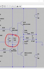
It depends on the exact amp design. For this one you could replace the 220 ohm with two series connected 100 ohms and connect the junction of these to the main output line to restore overall feedback.
What would be the wattage of these resistors i.e. what would a typical current through a driver transistor be?
Normally it would be very low indeed. Remember you only need about 0.6 volts across those resistors to begin to bias the outputs on and so that would be a wattage of 3 to 4 milliwatts.
Current would 0.6/100 which is 6 milliamps.
So very very low indeed.
The driver transistor current mainly flows into the base of the output transistor, not the resistor. Even a 1 amp driver transistor current flowing would still only see a little more than 0.6 volts across the 100 ohms and so still very low wattage.
The driver transistor current mainly flows into the base of the output transistor, not the resistor.
OK, but in a case of a "fully blown" channel like in this thread - how to stress test the driver transistors with the full load they will be handling during amplifier use before actually connecting the output transistors?
The idea behind this kind of stress testing is to "vaporize" the potential fake replacement transistors without taking the output transistors with them.
The easiest way is simply to make sure you use genuine parts from authorised distributers... fakes shouldn't even be a consideration really 🙂
However if you want to play then you have to make some ball park assumptions such as what the maximum driver transistor current might be, and that will depend on the gain of the output devices.
Lets say it is 200 milliamp peak and the amp can normally deliver 28 volts rms into 8 ohms which is 100 watts rms. The peak voltage is 28 * 1.414 which is 39 volts.
So you need a load that draws that current at 39 volts peak which would be 195 ohms.
The 100 ohm's I suggested earlier would now need to be a lot lower, say 10 ohm and you would need to alter the bias generator setting to be sure they were not conducting heavily.
Doing all that would let the amp deliver -/+35 volts into the now 195 ohm load and would pull a peak current of 200ma through the drivers.
The current gain of the output transistors would make a massive difference though. Low gain ancient parts could easily pull 200 or 300ma, maybe more while modern high gain parts could be under 100ma.
Doing all that would let the amp deliver -/+35 volts into the now 195 ohm load and would pull a peak current of 200ma through the drivers.
Where would that 195 ohm load resistor be connected?
Perhaps you could post a spice schematics for this kind of testing - things would be clear for a lot of readers after that 😉
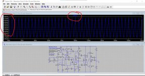
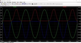
Like this. 35 volts peak across the 195 ohm load and approx 200ma peak driver current. No outputs fitted.
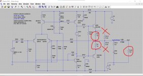
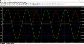
Third image is back to original spec and with modern high gain outputs fitted and the last image is with 2N3055/2955 types fitted which are much lower gain. You can see the differences in drive current between these devices and also how well the high load impedance and no outputs fitted simulation comes to approximating the operating conditions.
Third image is back to original spec and with modern high gain outputs fitted and the last image is with 2N3055/2955 types fitted which are much lower gain. You can see the differences in drive current between these devices and also how well the high load impedance and no outputs fitted simulation comes to approximating the operating conditions.
Attachments

Hi all,
I am back, and I managed to finally dial in the bias of my SONY TA-3650 amp. Hooray! And again huge gratitude to Mooly. You steered me through this and made it a great learning experience. I have much more confidence now to tackle the next machine waiting on the top of the pile (a Sansui TR-707 receiver).
I needed to find the right ratio between R1 and R2, the two parts of the resistor in both sides of the wiper in the new preset on the rubber diode. Then I could set the bias with the "old" presets RT301/351. Those are pretty coarse, the bias shoots up at one point. It really helps to have the rubber diode presets. thanks, Mooly, for insisting to use a pot here. Probably it would be safest now to change RT301/351 to a fixed value.
Work left is replacing the custom double can filter cap, as the amp is supposed to work for a while now, and the person I'll give it to won't be able to do maintenance work. So some more surgical work, as I'll need to replace the cap with two single ones and then build an adaptor PCB or some other construction. I admit I'd love to send off the machine now!
As to the sound... I am happy. I'd say it still has the very detailed and somehow typical (think STR-6060) early SONY treble. Nice phono section too, with the FET input stage. Pretty powerful. I am hopeful my brother in-law will be satisfied. I'll give him a pair of recapped DUAL CL-180 speakers and an equally refurbished Philips CD player (TDA1541) with it.
Thanks again, Mooly. And I am sure everybody who reads this tutorial will have as much fun as I did, and I assume Mooly as well.
PS the date on the pic in my electronics diary is not the day I finished the repair... which was yesterday 🙂 Had to finish two major works and was abroad for 6 weeks...
PPS edited for spelling reasons
Attachments

Last edited:
Thanks for all the kind words 🙂 and I'm pleased it has all come good in the end. I seem to remember thinking (without re-reading it all) that the 'rubber diode' would be pretty device critical and that making it adjustable would be best.
Sound like you have done a great job in refurbing it all
Sound like you have done a great job in refurbing it all
- Home
- Amplifiers
- Solid State
- Sony TA-3650 power rail resistors burn