Very cool 😎
An interesting property, I've noticed in a number of the current-driven VAS designs over the time - ULGF may be rather low (600-800KHz) - however, step response is very fast, the slew rate is more than just good.
An interesting property, I've noticed in a number of the current-driven VAS designs over the time - ULGF may be rather low (600-800KHz) - however, step response is very fast, the slew rate is more than just good.
Yes, the low ULGF is a useful feature. High ULGFs can sometimes spell danger.
Another feature is how well the VAS performs at large voltage swings. The THD doesn't increase as quickly as you would expect. Even close to clipping the THDs are still decent.
As far as my tribute to VHex goes, I'm not completely happy with the casodes at the front end. I'd like to give the input Jfets more voltage. Therefore, allowing higher voltage rails to be used. Make it scaleable. But I do like the elegance of the current design.
Observation
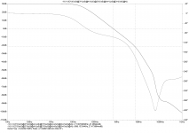
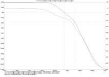
Loop gain at 0V, +31V and -31V.
0V
ULGF = 689KHz
PM = 82 Degrees
GM = 22dB
+31V
ULGF = 573KHz
PM = 76 Degrees
GM = 20dB
-31V
ULGF = 640KHz
PM = 78 Degrees
GM = 21dB
The amount of feedback stays fairly constant despite output level. Previous designs of mine have slowed down much more significantly at high output voltages.
Paul
Attachments

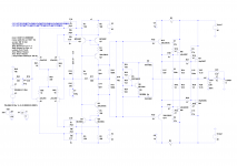
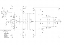
Thanks. I was missing something. Had overlooked R14 tied to 'out'. Eyesight not what it used to be. All clear now.In this design, there are three main loops:
1) Global Feedback Loop (R14)
2) VAS/IPS Local Feedback Loop (R12 + R13)
3) MIC Loop (C2 + C13 then through R11)
Paul
The amount of feedback stays fairly constant despite output level. Previous designs of mine have slowed down much more significantly at high output voltages.
Paul
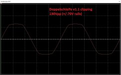
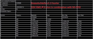
Right - it can be also noticed when measuring THD, sweeping the output level up to clipping - THD stays low up to very high swings, starting to raise right before clipping itself.
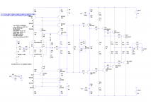
Another Version
This one has a few less active devices and lower front end bias currents but has almost identical performance. Also, added some current limiting.
Paul
This one has a few less active devices and lower front end bias currents but has almost identical performance. Also, added some current limiting.
Paul
Attachments
Last edited:
Hi Valery,
Alternative way of driving the current mode VAS...
What do you think? Potential?
Paul
Hi Paul, in fact this VAS configuration has got more potential than I could think of 😀
This configuration looks interesting - those transistors Q8, Q9 were initially aimed to provide the voltage reference for keeping the VAS in constant voltage conditions, however - you can drive the right side of the mirrors through them - no problem 🙂
Must be a rather fast one.
Apologies for the rambling
Hi Valery,
Glad you think this has potential. It is quite an efficient design in that the jFETs serve two purposes - "self biasing" the IPS and biasing the VAS. One advantage to this is that the PSRR of the input stage is massively improved. Haven't worked out how to do simulate this in LTSpice yet but you can pretty much change the supply voltages to whatever you want and the bias currents stay almost the same.
Moving the jFETs to inside the VAS has another advantage. They now see a much lower voltage. Hence, lower power dissipation and less thermal issues. So now the design can easily be scaled. No need for any cascodes now.
One area up for debate is the best way to drop the voltage to the jfets.
1) Plain resistors - this works surprisingly well. Square waves are fast and clean. The penalty is that the higher the value of resistor the greater the stability sacrificed. Although, this is pretty small in simulation. Bypassing the resistors with small capacitors (of the order of a few 10s of nF) solves this issue. Although the loop gain increases towards DC. Think this may be down the resistors being unaided at low frequencies. Or maybe I messed up something in the simulation??..
2) Zeners - The lower impedance works wonders. Bypass capacitors only required for noise purposes. Noise, obviously, is the disadvantage here.
3) Vbe multipliers - work well but higher part count.
Which would you go for?
The next point is an observation. The ULGF is almost static from 0V to the onset of clipping. This design is the best I have seen so far for this. The only thing that changes slight is the stability. Loss of GM is main effect.
Linearity is superb. This design runs just under 30dB of feedback with a ULGF of around 600KHz and still gets reasonable distortion figures.
As for speed, it slews at around 80V/us with BJT output stage. No sign of cross-conduction even from rail to rail. Maybe should try it with a vertical MOSFET output stage. Would be interesting to see the PM/GM/ULGF with MOSFETs...
Where next? We are a long way from the classic blameless here. 😉
Thanks for sharing your inspirational ideas 🙂
Paul
Last edited:
I have a new addition to the VHex family up and running today. The Lichtstark-X is running smoothly and awaiting more in depth testing. It seems rock stable so far. DC offset remains within a couple mV. Clipping is nice. Another great design by Valery. I need to get a second channel running yet and give it a listen.
Attachments
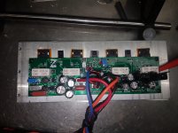
I have a new addition to the VHex family up and running today. The Lichtstark-X is running smoothly and awaiting more in depth testing. It seems rock stable so far. DC offset remains within a couple mV. Clipping is nice. Another great design by Valery. I need to get a second channel running yet and give it a listen.
Thank you Jeff! The board looks great - another VHex+ compatible footprint ))
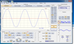
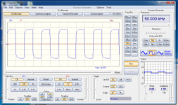
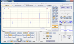
Nice clean squares with rather high slew rate and well-shaped corners (no overshoot whatsoever), plus clean clipping. The front-end justifies its name 😉
Looking forward to your listening tests - expecting highly natural sound 😎
Good example of the right wiring approach for a power amp - fat wires for the rails, ground and output are close to each other. Perfect!
Where next?
Hi Paul
Nice to see more of your ideas.
I would be interested to see a loop gain plot for the path after the two feedback paths join, that is, to the left of the junction point.
Best wishes
David
Hi Valery,
Glad you think this has potential. It is quite an efficient design in that the jFETs serve two purposes - "self biasing" the IPS and biasing the VAS. One advantage to this is that the PSRR of the input stage is massively improved. Haven't worked out how to do simulate this in LTSpice yet but you can pretty much change the supply voltages to whatever you want and the bias currents stay almost the same.
Moving the jFETs to inside the VAS has another advantage. They now see a much lower voltage. Hence, lower power dissipation and less thermal issues. So now the design can easily be scaled. No need for any cascodes now.
One area up for debate is the best way to drop the voltage to the jfets.
1) Plain resistors - this works surprisingly well. Square waves are fast and clean. The penalty is that the higher the value of resistor the greater the stability sacrificed. Although, this is pretty small in simulation. Bypassing the resistors with small capacitors (of the order of a few 10s of nF) solves this issue. Although the loop gain increases towards DC. Think this may be down the resistors being unaided at low frequencies. Or maybe I messed up something in the simulation??..
2) Zeners - The lower impedance works wonders. Bypass capacitors only required for noise purposes. Noise, obviously, is the disadvantage here.
3) Vbe multipliers - work well but higher part count.
Which would you go for?
The next point is an observation. The ULGF is almost static from 0V to the onset of clipping. This design is the best I have seen so far for this. The only thing that changes slight is the stability. Loss of GM is main effect.
Linearity is superb. This design runs just under 30dB of feedback with a ULGF of around 600KHz and still gets reasonable distortion figures.
As for speed, it slews at around 80V/us with BJT output stage. No sign of cross-conduction even from rail to rail. Maybe should try it with a vertical MOSFET output stage. Would be interesting to see the PM/GM/ULGF with MOSFETs...
Where next? We are a long way from the classic blameless here. 😉
Thanks for sharing your inspirational ideas 🙂
Paul
Hi Paul,
Took some time for me to think 🙂
There's one more option for "the best way to drop the voltage to the jfets" - cascode with bjts like ksc1845/a992 - the one I like the best. Slight parts count increase, but high scalability for almost any rails / output swing required without sacrificing stability. Agree?
With regards to what's next - I have good results, experimenting with multiple feedback loops, see the feedback arrangement in Sauberkeit-LT IPS. Another advantage of that kind of topology - the first voltage gain stage can run at low rails, being scaled-up at the next stage with the mirrors.
So, the idea now - replace the OpAmp with a simple discrete circuit, based on your self-biased jfet-based IPS. I will show you my option, demonstrating extremely promising results.
By the way, I have arranged soft-clipping in this "discrete OpAmp", resulting in very tube-like rounded shape even in deep clipping conditions.
I think - this is the way to go next 😉
Cheers,
Valery
Hi Paul
Nice to see more of your ideas.
I would be interested to see a loop gain plot for the path after the two feedback paths join, that is, to the left of the junction point.
Best wishes
David
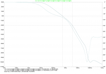
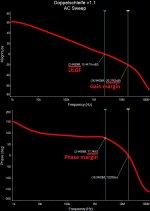
Hi David,
Hope it may be of interest for you - here are a few simulation results of what I have just described to Paul in the message above. Feedback loop analysis is performed in combination with NS Modular OPS, showing the "right" loop, covering OPS.
Expect an email 🙂
Cheers,
Valery
Attachments
Nice JeffI have a new addition to the VHex family up and running today. The Lichtstark-X is running smoothly and awaiting more in depth testing. It seems rock stable so far. DC offset remains within a couple mV. Clipping is nice. Another great design by Valery. I need to get a second channel running yet and give it a listen.

A good combination of smd and through hole parts.
Yes, Valery is one of the best designer in the forum!
He is kind enough to explain everything if someone ask.
Thanks Valery!
Hope it may be of interest for you - here are a few simulation results of what I have just described to Paul...
Thanks Valery, it is a pity that you don't use LTspice because I am not sure how your loop gain plots compare to a Tian probe.
I expect they are equivalent to first order, but it is precisely the "non-ideal" behavior that interests me, that was what I wanted to study in Paul's example.
Could you show where you measured loop gain on your circuit?
Best wishes
David
Last edited:
Hi Paul
Nice to see more of your ideas.
I would be interested to see a loop gain plot for the path after the two feedback paths join, that is, to the left of the junction point.
Best wishes
David
Hi David,
Good to hear from you again.
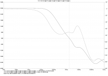
The design has evolved slightly so have attached the schematic and the .asc file.
Here are a couple of plots of loop gain for you. The first is the global loop and the second is the probe positioning requested.
Outer loop looks good before the join but after looks like it could do with some tweaking.
Hopefully this can be another educational episode 🙂
Paul
Attachments
Hi Paul,
Took some time for me to think 🙂
I think - this is the way to go next 😉
Cheers,
Valery
Hi Valery,
Thank you for your feedback and suggestions. They have already stimulated one "inspiration". 🙂
Need some time to process your ideas too. 😉
Thank you!
Paul
...but after looks like it could do with...
It does look pretty stable however, and this was my main interest.
Theory says the outer loop stability should track that loop that I asked about and this seems to be true, all is fine.
I have also started to experiment with FET IPS but simpler than yours, CFA not LTP. Will post after I finish a bit more work.
Best wishes
David
Hi David,
Yes, stability margins are good. But then as you say the theory says it should be. My thinking was that as it shares the same compensation as the outer loop but with less transistors (fewer poles) then "by default" it should have better margins.
Have managed to tidy up the phase response by changing the compensation on the driver bases. Just needed to add a zero in.
Will post some plots etc. when at home.
A new question has surfaced in my mind. Do I need a CMCL? There may be undefined voltages on the bases of the VAS output cascodes. A basic CMCL is used on a current mirrored Jon Curl style IPS (which is very similar). Need to look into this a bit more.
Look forward to seeing you circuit. I expect it will be highly optimised. 😉
Paul
- Home
- Amplifiers
- Solid State
- Sons of VHex