Didiet78,
You can share your pdf files, someone will find it useful as a personal build or for reference. 😉
Didiet & Bangla H,
 for keeping the Spirit of DIY.
Regards,
Albert
You can share your pdf files, someone will find it useful as a personal build or for reference. 😉
Didiet & Bangla H,
for keeping the Spirit of DIY.Regards,
Albert
Inspired by VHex 1.1 board i have tried a redesign for single Input.
Thank you very much for the Diptrace files.
Bangla - good work! There are a few things to correct though 😉
A good style of designing the boards in Diptrace is to keep the layout and the schematic in sync all the time - probability of some mistake will be minimized. Then you can go, in the menu - Verification -> Compare to schematic, and point to the file with schematic - you will see if something does not match.
Then, you can click File -> Renew layout from schematic -> By components, and also point to the file with schematic - Diptrace will update the layout - if some new parts are found, it will place them on the right from your layout.
Cheers,
Valery
Diptrace menu- renew
Thanks for help in more fine details Valery. 😛
Have seen in menu, but not used- now well.
With sort my own parts in comfortable library i have some difficulties in moment.
The most PCB design work was much better done from other members- i could
learn by viewing 🙂 and try do in little same way.
It is more to learn in tracing, create copper area....so on, but fun.
Gannaji, please share your layout work- we
thanks and fully agree abetir.
I have started correction, like advised.😉
.
A good style of designing the boards in Diptrace is to keep the layout and the schematic in sync all the time
Thanks for help in more fine details Valery. 😛
Have seen in menu, but not used- now well.
With sort my own parts in comfortable library i have some difficulties in moment.
The most PCB design work was much better done from other members- i could
learn by viewing 🙂 and try do in little same way.
It is more to learn in tracing, create copper area....so on, but fun.
Gannaji, please share your layout work- we
.for keeping the Spirit of DIY
thanks and fully agree abetir.
I have started correction, like advised.😉
.
Attachments
With sort my own parts in comfortable library i have some difficulties in moment.
Diptrace handles your custom parts in a smart way - you can specify your own patterns while you are in schematic view. In this case, each time you update the layout from schematic, it will use those custom parts, specified earlier.
Dear Valeri,
The feedback resistors at 27k/1k seem to be high by an order of magnitude. Any specific reason ?
gannaji.
The feedback resistors at 27k/1k seem to be high by an order of magnitude. Any specific reason ?
gannaji.
Dear Valeri,
The feedback resistors at 27k/1k seem to be high by an order of magnitude. Any specific reason ?
gannaji.
Hi Gannaji,
You're right - the lower impedance feedback network will lead to reduced distortion in 10...20KHz region, however - it will reduce the stability margins, requiring additional attention for keeping it stable. There is a number of ways to overcome this limitation, however I tried to keep the circuit as simple as possible for the moment.
Cheers,
Valery
Sunday afternoon play...
Has it been done before?
Valery's ideas used here. 🙂
I like it! Excellent use of my current-driven enhanced cascoded VAS 😉
I'm sure it's going to show very good overall performance.
Double-bootstrapped pre-drivers - a cool move as well.

Last edited:
Lichtstark
Paul, I did some further playing with the current-driven VAS as well - see the front-end design here.
I think - bearing in mind rather high-impedance NFB - the overall principle has fantastic potential 😎
Cheers,
Valery
Sunday afternoon play...
Has it been done before?
Valery's ideas used here. 🙂
Paul, I did some further playing with the current-driven VAS as well - see the front-end design here.
I think - bearing in mind rather high-impedance NFB - the overall principle has fantastic potential 😎
Cheers,
Valery
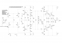
Here's a MOSFET version. Changed input cascode configuration as well.
No sign of cross conduction with square waves going close to the rails.
Well behaved, very stable and fast... 🙂
Paul
Paul, this one is fantastic! ))
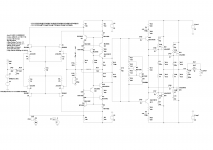
In principle, its front-end is somewhat similar to the jFET version of X4 design - VAS output stage consists of two symmetric current mirrors, driven from IPS collectors at 4 points:
X4 front-end with jFETs at the input
In X4 I'm running the IPS from +/-15V regulators, using 4 intermediate mirrors for driving the VAS main mirrors. Your arrangement is even better - common gate cascodes, plus more precise cascoded VAS mirrors - this is a front-end designer's dream 😀
This is the Lichtstark-Xdrive 😎
Worth prototyping and testing with both - this kind of HexFET OPS, as well as with NS Modular (needs to be layed out as a snap-on IPS module with standard connectors for this).
I can share a Diptrace template with you, where connectors are already in place, if you'd like to try.
In any case - thank you! This kind of ideas exchange moves us forward 🙂
Cheers,
Valery
Last edited:
Hi Valery,
Exchange of ideas is the main reason of posting this design. Glad this one has been of use. 🙂
Like you, I have grown a little weary of the standard blameless design. There has to be something a little out of the ordinary to keep me interested. Hence, my interest in your current drive VAS ideas.
The X4 design was an inspiration for this design. The 4WD aspect seems neat in that it makes use all the front end potential.
Compared to your Lichtstark variant, this one probably can't compete on THD terms but should be a match for the rest. It does satisfy those that like FET front ends. It can probably be optimized a little better and decision to be made whether to go DC servo or not. Ie. Should the feedback network be of higher impedance?
One little subtlety in this design is the positioning of the "speed up" caps on the MOSFET outputs. This allowed a lower driver bias and so far has eliminated cross conduction. Should work in reality. What do you think?
I'm up for doing a diptrace version 🙂 Only thing is the selection of the JFET inputs. The LSK/LSJ combination is very expensive. There is the option of going for MMBF**** SMD JFETS. These are cheap but need to figure out a jig for selection / matching. Have you any suggestions for this? The IPS bias current is not critical in this design. Would be good to setup the JFET cascodes so that a reasonable rail voltage can be used.
Can post further plots and specs if you are interested.
Paul
Am I missing something? (I admit not having read all 44 pages of this thread). I see that the NFB point is taken from the VAS, not from the output as is usually the case. Could someone please enlighten me why that has been done? To me this appears as though the OP stage is operating open loop, buffering the signal from the VAS. It is a voltage follower configuration, so the added distortion isn't a huge deal, but still.
(No offense intended to anyone - just a bit puzzled).
(No offense intended to anyone - just a bit puzzled).
Hi Valery,
Exchange of ideas is the main reason of posting this design. Glad this one has been of use. 🙂
Like you, I have grown a little weary of the standard blameless design. There has to be something a little out of the ordinary to keep me interested. Hence, my interest in your current drive VAS ideas.
The X4 design was an inspiration for this design. The 4WD aspect seems neat in that it makes use all the front end potential.
Compared to your Lichtstark variant, this one probably can't compete on THD terms but should be a match for the rest. It does satisfy those that like FET front ends. It can probably be optimized a little better and decision to be made whether to go DC servo or not. Ie. Should the feedback network be of higher impedance?
One little subtlety in this design is the positioning of the "speed up" caps on the MOSFET outputs. This allowed a lower driver bias and so far has eliminated cross conduction. Should work in reality. What do you think?
I'm up for doing a diptrace version 🙂 Only thing is the selection of the JFET inputs. The LSK/LSJ combination is very expensive. There is the option of going for MMBF**** SMD JFETS. These are cheap but need to figure out a jig for selection / matching. Have you any suggestions for this? The IPS bias current is not critical in this design. Would be good to setup the JFET cascodes so that a reasonable rail voltage can be used.
Can post further plots and specs if you are interested.
Paul
Paul - please post further plots and specs 🙂
With regards to jFET complements for the input stage - I consider K246/J103 an an option - they are much less expensive than LSK/LSJ, still available and complementary enough. What do you think?
Cheers,
Valery
More Details
This is a slightly revised version. Decided for simplicity to go for a higher impedance feedback network. This involved re-jigging the compensation. But the end result is a DC servo is not necessary and a smaller feedback cap is required.
Valery's suggested JFets work fine in this design. Again a small change in compensation was required for these.
JFet Models used:
.model J2sk246 NJF(Beta=1.07m Rs=56.76 Rd=56.76 Betatce=-.5 Lambda=2.8m
+ Vto=-2.638 Vtotc=-2.5m Cgd=10.38p M=.4373 Pb=.3905 Fc=.5
+ Cgs=6.043p Isr=112.8p Nr=2 Is=11.28p N=1 Xti=3 Alpha=10u Vk=100
+ Kf=1E-18 Af=1)
.model J2sj103 PJF(Beta=2.197m Rs=76.76 Rd=76.76 Betatce=-.5 Lambda=735.3u
+ Vto=-2.037 Vtotc=-2.5m Cgd=18.95p M=.5045 Pb=.3905 Fc=.5
+ Cgs=17.02p Isr=38.48f Nr=2 Is=3.848f N=1 Xti=3 Alpha=10u Vk=100
+ Kf=1E-18 Af=1)
Found elsewhere on this site. Not sure if they are any good. Does anyone have better models?
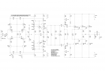
Some plots for the LichtStark 4WD...
1) Schematic
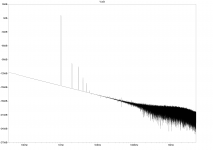
2) Loop Gain Plot
PM: 82 Degrees
GM: 22 dB
ULGF: 698KHz
This design does accept a lead cap over the feedback resistor. So it should be possible to make the ULGF somewhat higher.
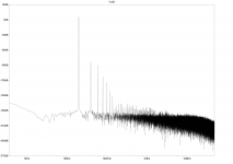
3) FFT 2.83V/8R/20KHz
THD = 0.003829%
4) FFT 2.83V/8R/1KHz
THD = 0.000686%
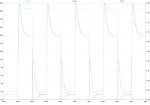
5) 100Khz Square Wave
6) Clipping - Absolute clipping level can be adjusted.
This design is only 24 hours old. Many improvements may be possible. Any suggestions welcome. 🙂
Paul
This is a slightly revised version. Decided for simplicity to go for a higher impedance feedback network. This involved re-jigging the compensation. But the end result is a DC servo is not necessary and a smaller feedback cap is required.
Valery's suggested JFets work fine in this design. Again a small change in compensation was required for these.
JFet Models used:
.model J2sk246 NJF(Beta=1.07m Rs=56.76 Rd=56.76 Betatce=-.5 Lambda=2.8m
+ Vto=-2.638 Vtotc=-2.5m Cgd=10.38p M=.4373 Pb=.3905 Fc=.5
+ Cgs=6.043p Isr=112.8p Nr=2 Is=11.28p N=1 Xti=3 Alpha=10u Vk=100
+ Kf=1E-18 Af=1)
.model J2sj103 PJF(Beta=2.197m Rs=76.76 Rd=76.76 Betatce=-.5 Lambda=735.3u
+ Vto=-2.037 Vtotc=-2.5m Cgd=18.95p M=.5045 Pb=.3905 Fc=.5
+ Cgs=17.02p Isr=38.48f Nr=2 Is=3.848f N=1 Xti=3 Alpha=10u Vk=100
+ Kf=1E-18 Af=1)
Found elsewhere on this site. Not sure if they are any good. Does anyone have better models?
Some plots for the LichtStark 4WD...
1) Schematic
2) Loop Gain Plot
PM: 82 Degrees
GM: 22 dB
ULGF: 698KHz
This design does accept a lead cap over the feedback resistor. So it should be possible to make the ULGF somewhat higher.
3) FFT 2.83V/8R/20KHz
THD = 0.003829%
4) FFT 2.83V/8R/1KHz
THD = 0.000686%
5) 100Khz Square Wave
6) Clipping - Absolute clipping level can be adjusted.
This design is only 24 hours old. Many improvements may be possible. Any suggestions welcome. 🙂
Paul
Attachments
-
 LichtStark 4WD Schematic.png115.1 KB · Views: 490
 -
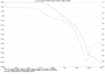 LichtStark 4WD Loop Gain.png79.3 KB · Views: 456
 -
 LichtStark 4WD FFT20.png76.2 KB · Views: 390
 -
 LichtStark 4WD FFT1.png60.2 KB · Views: 133
 -
 LichtStark 4WD 100KHz SQ.png105.5 KB · Views: 143
 -
 LichtStark 4WD Clipping.png84.6 KB · Views: 140
 -
LichtStark 4WD.asc14.7 KB · Views: 166
Am I missing something? (I admit not having read all 44 pages of this thread). I see that the NFB point is taken from the VAS, not from the output as is usually the case. Could someone please enlighten me why that has been done? To me this appears as though the OP stage is operating open loop, buffering the signal from the VAS. It is a voltage follower configuration, so the added distortion isn't a huge deal, but still.
(No offense intended to anyone - just a bit puzzled).
The two resistors you are talking about are a local loop around the VAS and IPS. They allow the limiting of global loop gain by using it to linearise the front end (Can also improve stability margins). The also allow the VAS output impedance to be accurately defined and made lower. This has the effect of swamping the distortions caused by the non linear loading of the drivers.
In this design, there are three main loops:
1) Global Feedback Loop (R14)
2) VAS/IPS Local Feedback Loop (R12 + R13)
3) MIC Loop (C2 + C13 then through R11)
(Drawing from post 434)
Valery may be better placed to explain the intricacies of the VAS loading resistor...?
Paul
- Home
- Amplifiers
- Solid State
- Sons of VHex