I recommend that when you put together an equation which spits out a value for R_high_and_okay, you should definitely include a term with the DC bias current drawn by the amplifier (from the supply), with no input signal and no output signal.Do you have any guidance on arriving at a "too high" added resistance?
Class-A amplifiers such as the Nelson Pass A40 (20 watts/channel @ 8R), or the Thagard/Pass A75 (75 watts/channel @ 8R), send their startup current to two different places: firstly, to charge up the power supply filter capacitors. Secondly, to run huge DC currents in the output predriver and driver transistors. You will want to choose R_high_and_okay, keeping in mind that when your time delay relay shorts it out, the current drawn from the secondary (and thru the primary fuse) will include both the class-A bias current AND the remainder of the capacitor charge-up current.
This is much less significant in Class-B and low bias Class-AB amplifiers.
 split from the diyaudio store and moved to psu section so as to give this thread more exposure...
I have no idea what would go into that equation. That's why I asked if you have any guidance to offer?I recommend that when you put together an equation which spits out a value for R_high_and_okay, you should definitely include a term with the DC bias current drawn by the amplifier (from the supply), with no input signal and no output signal...................
I offer the suggestion that your equation should NOT omit "DC bias current drawn by the amplifier"; otherwise you will get the same resistance value for Class-B amplifiers and Class-A amplifiers, which would be nonsense. Even Rod Elliott (who supplies paragraphs of text recommendations instead of an equation) mentions the need for different inrush current resistances in classes B and A.
I offer a second suggestion that the timing of the soft-start-disengage relay opening, is significant. Proof: imagine scenario A in which the relay disengages after 10 milliseconds (1/2 of an AC mains period), and imagine scenario B in which the relay disengages after 500 milliseconds (25 AC mains periods). Do scenarios A and B apply equal stresses upon the transformer, diodes, capacitors, and fuses? (answer: no). Thus your equation for calculating R_high_and_okay needs to include relay timing in some form or another.
I offer a third suggestion that the capacitance (in Farads) charged by the rectifiers, is significant; and it belongs in your equation that calculates R_high_and_okay.
I offer a fourth suggestion, that the transformer VA rating probably does not need to be included in the equation for R_high_and_okay. You already use it to calculate R_low_and_okay; I doubt that you need to use it when calculating a resistor that stresses the transformer less rather than more.
If you are allergic to the word equation, perhaps it will make you feel better to substitute the word procedure.
Last edited:
Varistors are a good fit for Class A. Not so much for AB or D. They need continuous current draw to stay low impedance. The common CL60 device has a stated range of 1.2 to 5.0 Amps. Less than 1.2 amps and the core slug cools off and the resistance starts to rise again. Over 5 and self-heating becomes a problem. Remember that even when hot, the resistance doesn't go to zero. At 5 amps continuous draw the series resistance is 0.18 ohms. Why strive for milliohm connections when you leave the CL60 in there? I still prefer to bypass them with a relay.
Bill, if you bypass the Inrush Current Limiter (CL60 et al) with a relay, doesn't that guarantee it'll work equally well for all classes of amplifier biasing?Varistors are a good fit for Class A. Not so much for AB or D ... I still prefer to bypass them with a relay.
Mark,
Yes. I was implying varistors by themselves are best suited for Class A. Bypassing them makes for a more universal circuit that isn't limited to a 4 to 1 current range.
There are other benefits to bypassing them. A momentary interruption will find the thermistor in its cold state and able to do its limiting. Also bypassed they will run cool. Otherwise they will be at 150 °C or more if the idle current is high.
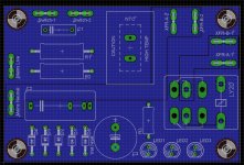
I had a play around with a board layout for the soft start design we've been kicking around - the one which makes use of a big fat NTC ICL. As my project has two transformers, I wanted two sets of output connectors. Annoyingly I couldn't get the connections for each transformer next to each other because of the criss-crossing required; instead the two 'live' are adjacent and the two 'neutral' adjacent. I'm still poking around with it but if anyone has suggestions I'd gladly hear them. The board is 6x9cm (mounting holes on 1cm grid).
Attachments

Last edited:
In case not obvious, each pic is with the bottom or top layer turned off, respectively. It's not a pic of the top and bottom of the board.
Hi, I think it would be a very good idea to do some research on AC mains safety regulations. Two words to look up are "creepage" and "clearance". Here are a couple of links but I don't know whether these are the best or the worst on the internet.
(link 1) .... (link 2) .... (link 3) .... (link 4)
Your PCB layout appears to place live AC mains traces, rather near to other things. Maybe this isn't a good idea.
(link 1) .... (link 2) .... (link 3) .... (link 4)
Your PCB layout appears to place live AC mains traces, rather near to other things. Maybe this isn't a good idea.
OK - thanks a lot So greater clearance for all mains voltage traces and components. The links you provided and a few others from Google point to same/similar calculators. If I plug in 350V peak I get 2.5mm for IPC-2221B external, 0.8mm for coated and 2.3mm for IPC 9592. I've not yet been able to find out what constitutes "coated"? Is a Hasl finished PCB "coated" in the sense these calculators mean? Clearances of near 100mil will be difficult to achieve when the pins of the DPDT switch are only a fraction over 75mil apart. Perhaps that's a reasonable benchmark to use.
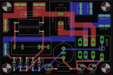
Revised draft attached. (25mil grid albeit hard to see it clearly with this snip.) Perhaps still some issues in top right quadrant (eg XFR-A-1 Faston distance from the trace from the NTC). Maintaining large separation at the relay pins is challenging if the trace is to envelop the pin. Necessary?
A related question regarding thermals: is it better to turn them off for the high current trace connections? (i.e. Fastons, NTC and relay). Off with narrower trace (which doesn't envelop the pin)?
I changed C2 to provide for larger 27.5mm pitch caps. Perhaps I can drop accommodation of 15mm pitch.
A related question regarding thermals: is it better to turn them off for the high current trace connections? (i.e. Fastons, NTC and relay). Off with narrower trace (which doesn't envelop the pin)?
I changed C2 to provide for larger 27.5mm pitch caps. Perhaps I can drop accommodation of 15mm pitch.
Attachments

Last edited:
Why is all unoccupied PCB area "filled" (maybe your software calls it "flooded")? Is the filled/flooded area electrically [special=]%[/special]floating, or is it connected to a circuit node? By design the circuit has no transformer to provide isolation; every single node of the circuit is derived from the AC mains. The deadly AC mains.
I might be especially concerned about the filled area surrounding the mounting holes. Over time, as the solder mask insulation abrades away, the mounting fasteners could eventually short to the fill, making the fastener bolt/nut/washer "live" (a danger to service personnel), and possibly shorting to the chassis.
I might be especially concerned about the filled area surrounding the mounting holes. Over time, as the solder mask insulation abrades away, the mounting fasteners could eventually short to the fill, making the fastener bolt/nut/washer "live" (a danger to service personnel), and possibly shorting to the chassis.
I just did a ground plane (top and bottom). Sounds like that's not a good idea here - damage could lead to the ground plane being connected directly to the mains.
Re the mounting holes, The inner circle of 3.2mm diameter is the drill hole. The outermost circle is the beginning of the ground pour (i.e. no copper inside the outer circle). Even with a washer the fastenings don't extend to the ground pour.
Re the mounting holes, The inner circle of 3.2mm diameter is the drill hole. The outermost circle is the beginning of the ground pour (i.e. no copper inside the outer circle). Even with a washer the fastenings don't extend to the ground pour.
I'd suggest you change the footprint and drill size of the zener diode, so your board can accommodate both the 1N4749 and the 1N5359 (24V, 5W); the board will work no matter which diode the purchasing agent happens to buy.
I'd also suggest putting a silkscreen "K" next to the cathodes of the 3 LEDs, in case your purchasing agent happens to buy LEDs that don't have a flat spot on the package. The boneheads at Lite-On sell quite a few LEDs whose only indication of polarity, is the length of the leads. Yes really.
Finally, I suggest you put something on the bottom side of the board (silkscreen? text-in-copper?) that indicates the polarity of the electrolytic capacitor. When the cap is inserted, it covers up the silkscreen marking on the top side of the board, so a reminder on the bottom side will reassure the assembly technician that she hasn't stuffed the capacitor backwards.
Attachments
Thanks Mark. I will make the first two changes tomorrow. Re the third, it's there already. (You can just make out the ghost of the + sitting on the bottom of the board more or less directly under the + on the top.) I took that from your earlier advice on other boards. 🙂
I have a question regarding trace widths and copper thickness. I have looked at a number of PCB trace width calculators, in particular this one. They would suggest that for 5A continuous and 1oz copper, 109mil is fine. I conclude that the 150mil or so traces for the main currents on this board should be more than enough. Is it really necessary to go to 2oz copper?
If anyone else has suggestions to improve the board please let me know.
Here's what I got (in blue). I used THIS online calculator.
I installed a couple of margins-of-safety (in red).
I installed a couple of margins-of-safety (in red).
Attachments

Thanks for the link to the calculator. Better than the one I was using. 2oz copper it is.
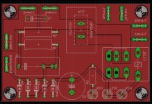
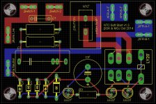
Pic of penultimate (maybe) version attached. D5 lengthened to accommodate a 1N5359B. Cathodes marked. Silk added.
Anyone else have other suggestions?
(If anyone is interested in sharing the cost of a small production run please let me know.)
Pic of penultimate (maybe) version attached. D5 lengthened to accommodate a 1N5359B. Cathodes marked. Silk added.
Anyone else have other suggestions?
(If anyone is interested in sharing the cost of a small production run please let me know.)
Attachments
- What's the simulated power dissipation in your 1 Megohm, 3 watt resistor? If I've done the calculation correctly, you will need 1700 volts across that resistor to make it dissipate 3 watts.
- Please take my initials off the PCB. (a) It is your design; (b) I don't want some future person asking me for technical support.
- Home
- Amplifiers
- Power Supplies
- Soft start circuit design and other psu issues