Finally update with pictures of the repair.
Its not pretty but it seems to suffice
As I've tested positive for Covid this weekend I guess I'll find out in the next few days, once I start to feel less 'ugh'
Andy
Its not pretty but it seems to suffice
As I've tested positive for Covid this weekend I guess I'll find out in the next few days, once I start to feel less 'ugh'
Andy
Attachments
Ebay sources of J18/K60 need to be taken with some level of caution. While the parts themselves are genuine in most cases, the markings are not. In some cases you may get J28 marked as J18, or J82 marked as J60, but in most cases the rank code will not have much to do with actual rank.2sk60 and 2sj19 can be found on eBay. My supply was a gift from a diyer here who got them as a gift from Jim Bongiorno.
Note that the rank number is only the last digit of the production code. It is possible to check the rank but requires access to two lab power supplies, one for the source-drain circuit (60V current limited to about 200mA), the other for the gate-source bias (adjustable to 30V, only a fraction of a mA is required). The other way is within the amplifier, by installing only one pair of VFETs into the amp (of course, this is for measurement purposes without a load), and checking the gate voltages with appropriate idle current. Remember that the idle current should be adjusted to half the factory value since only half the VFETs will be installed, and under normal normal (ideal) conditions each VFET in parallel contributes half the total idle current. In this case we want to have the same idle current in the one installed par, so that's half of two pairs.
For each pair tested, you will have the gate voltage required for the N and P channel part. Check this for all VFETs (rank will not matter at this point since no VFETs are run in parallel), then select groups to go in parallel with the least difference in gate voltage.
For simplicity, the gate voltage itself is measured between the amp output terminal and the gate line (there are test pads on the PCB to do this!). This introduces a small measurement error, which is exactly the voltage in mV that is used to check idle current. However, since the gate voltage will be on the order of 10V (there is quite a variation depending on rank, some volts - lower ranks have a lower gate voltage) the error is negligible. Each channel has two of each VFETs in parallel, make sure to group the ones that go in parallel so the difference in gate voltage is as small as you can get it. Under the idle conditions in this amplifier, a gate voltage difference of around 1.7V is equal to one rank difference. The parallel VFETs should always be the same rank, as should be the opposing polarity VFETs, but in a pinch a difference of one rank between J and K is acceptable, the amp will have somewhat higher distortion figures, due to increased even order harmonics caused by the rank difference. Of course, this is for VFETs within one channel, different rank pairs can be installed in the other channel.
It is also worth noting that there is no particular reason to select for high rank VFETs in any of the first generation Sony VFET amps, but using them in the second generation amps like the TA-N7 and TA-F7 has advantages. Higher rank units will, however, result in an amplifier with lower distortion at high power output, so if your speakers are not very efficient and require the amp to be operated at a higher power output, it might be worth favoring ranks 6 or 7.

Sure, though it also requires a heatsink and adjustment on-fly, whereas using two power supplies needs only a second or two for binning.You can also test with a single supply using a Source resistor to ground, grounding the Gate, and measuring the voltage across the resistor.

The problem is that the only reliable table of Vgs (about 9 to 25V) that corresponds to the rank number is at Vds of 60V and Id of 177mA.
If it is down t just matching, for sure that can be done at a lower voltage but not too much lower - there should be at least some 30V across D-S to get reliable results... the problem in a single supply measurement setting is that a higher drop on the source resistor means a lower Vds, if the supply voltage is the same, and the VFET being essentially a semiconductor triode, both voltages move the VFETs working point. Also, the current at which the matching is done should be representative, i.e. at least on the order of the no-signal bias current through the VFET in the amp where it is going to be used in.
Alas, 7 of the 8 VFETs are dead, they led a happy life... also a couple of resistors look burned up in 1 channel. I am going through the board slowly to find the cause, I suspect the Double Diodes may the the root, probably taken out a few other parts along the way..Thanks Andy,
Will let you know if there is anything i am short of, but seller seemed totally genuine, amp arrived with original bill of sale from 1979 and the pristine copy of the handbook with the original power lead. Was very well packaged and it very clean. Will test the VFets and if they are good, will check the relay and work from there.
Fingers crossed there will be no smoke on you PA board.
I’ll upload some photos as I progress.
J
Now to find 4 matched pairs of VFETs at a reasonable price.
J
OOFAlas, 7 of the 8 VFETs are dead, they led a happy life... also a couple of resistors look burned up in 1 channel. I am going through the board slowly to find the cause, I suspect the Double Diodes may the the root, probably taken out a few other parts along the way..
Now to find 4 matched pairs of VFETs at a reasonable price.
J
Somethings done for both channels.. You're more able than I am, but somethings upset the PSU there? What a shame though.
I'll remind you that I did get rank 53 to work just fine, even though that's outside the original spec - it widens the pool a bit
Andy
sOOOOOOO YEAH about that repair...
Turns out I'm not 'OK' with repairing something I hope will be the definitive amp. Don't think there is much wrong with the repair, only the concept, feels like a fix...
At least one reason that this one has taken so long is that in my heart of hearts, I know it will be compromised by a bad board. The other being the TA-5650 that providing exactly no reason to replace it 🙂
Sometimes, I am my own worst enemy 😈
Put your feet up! this feels like it just got L.O.T.R. saga like.
Immediate question is do I test "wot I got" up to a point? or take all the bits out and test individually. Is there any merit in the former? The latter seems MUCH more boring...
You should not use the attached - its NOT checked (yet), also you will need some unobtanium parts... Feels like a high bar!! The new V-fet amps by Monsignor Pass are a much more sensible exercise. As I have said before, this thread is to document my own errors / progress rather than provide a manual. If my meandering commentary is of use, even if as a warning, then that's OK
Andy
Attachments
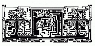
Nice PCB art work there.sOOOOOOO YEAH about that repair...
Turns out I'm not 'OK' with repairing something I hope will be the definitive amp. Don't think there is much wrong with the repair, only the concept, feels like a fix...
At least one reason that this one has taken so long is that in my heart of hearts, I know it will be compromised by a bad board. The other being the TA-5650 that providing exactly no reason to replace it 🙂
Sometimes, I am my own worst enemy 😈
Put your feet up! this feels like it just got L.O.T.R. saga like.
Immediate question is do I test "wot I got" up to a point? or take all the bits out and test individually. Is there any merit in the former? The latter seems MUCH more boring...
You should not use the attached - its NOT checked (yet), also you will need some unobtanium parts... Feels like a high bar!! The new V-fet amps by Monsignor Pass are a much more sensible exercise. As I have said before, this thread is to document my own errors / progress rather than provide a manual. If my meandering commentary is of use, even if as a warning, then that's OK
Andy
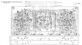
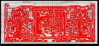
Thanks! But I've progressed from there. The original plan was just to scan from the paper service manual, tidy up and print, but then I had thoughts....Nice PCB art work there.
"AutoCAD" to the rescue (not a phrase often heard)
So it seems that Sony for the most part used a 2.5mm grid which makes life actually fairly simple > 8 hours later.... 😀
As this is now vector 'art' I can 'FIX' things, somewhat aware that the original 1975 draftsmen would have been in awe of the ability to just push a component along a pitch with just a click. Just as I am in awe at being able to create a board without it.
- First thing is that the bias pot on the right channel is sorta wonky, move it left 2.5mm and its as pretty as the left channel.
- I also thickened up / widened 'some' traces from 1mm to 1.5mm. Where possible that's been the route, again the right channel is more fiddly than the left.
- VD1221's, I've elected not to re do the board so that they genuinely become 2 x IN400x's. It's really only half simple on the right channel. and i'm pretty happy with the solution we've got
- The track passing between the thermistor's legs (PTH701)is offset requiring one pad to be compromised - not anymore.
- Now can I get the 10w 0.22ohm Mundorf resistors in there, the little cement blocks that were in there were truly grubby. Is there a 'hi-fi' version of these?
As for the Vfets who knew they were on a 30mm and 33mm alternating pitch 🙂
Not 100% sure on the rules, so I'm posting screen grabs in the knowledge they are useful for progress but that's it. If anybody wants AutoCAD files let me know, just have to figure out how to share.
Just need to scan the actual board to check for any Sony surprises - but progress! This was definitely the right way to go.
Andy
Attachments
Hi Andy,
“
VD1221's, I've elected not to re do the board so that they genuinely become 2 x IN400x's. It's really only half simple on the right channel. and i'm pretty happy with the solution we've got”
how are you going to thermally couple them to the driver transistor? The “botch” solution is simple with some compound and shrink tubing.
We have some board layout guys at work, doing 6+ layers… blows my mind as even 2 layers keeps me busy for a week.
Jon
Another good reason not to bother! You're right that the "botch" works. I have heard mixed 'opinions on the thermal coupling and not understanding it well enough have always leaned on; "If Sony did it, and not doing it would have saved money, its probably worth doing"how are you going to thermally couple them [VD1221 diodes's] to the driver transistor? The “botch” solution is simple with some compound and shrink tubing.
However, I'm mostly posting to confirm the board layout vs reality and show off my amazing 'press and peel' success with hindsight the "re-manufactured in England should have been GB" (Sorry Jon 😳)
Attachments

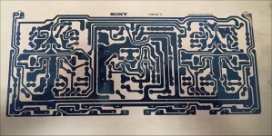
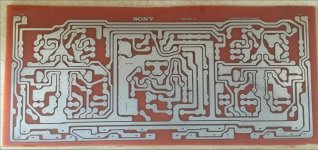
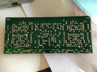
Now the joy of drilling all the holes…Board etched and tin plated!
Pride comes before a fall - this is never gonna work...
Andy

Ha Ha indeed, followed by the joy of 'oh missed one'Now the joy of drilling all the holes…
Genuinely, if anyone is looking for PCB drilling tips, get a drill press and some magnifying glasses (spectacles) so you can really see whats going on.
Andy
Worse! When foil from a pad wraps around a bit taking whole track sometimes. I would drill before hand if doable.Ha Ha indeed, followed by the joy of 'oh missed one'
SKIPPED
Andy
Not sure I follow, I drill all holes on the board first then check and check again - still miss ones where the pilot hole has gone AWOL. But if the whole track goes I'd consider it a bad board - still curse tho' that's how I got into this mess in the first place 🙂Worse! When foil from a pad wraps around a bit taking whole track sometimes. I would drill before hand if doable.
Meanwhile, all this fiddling has prompted capacitor questions.
Ceramic capacitors are 'BAD' (apparently they are not audiophile enough IIRC ) and I do have the option of stuffing whatever I like in the new board. These are decoupling the base on the (helpfully annotated) emitter follower 30pF
I have some 47pF polystyrene, is that an upgrade, or am I going down entirely the wrong rabbit hole. Any semiconductor ppl / actual electrical engineers care to help? (is that noob enough)
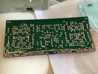
Finally, the board has been test fitted and components are going in, resistors and jumpers first...
Andy
Attachments

- Home
- Amplifiers
- Solid State
- So now its a V-FET trilogy