That is IT. Perfection.
ND has been built , greenamp is just the VFA version.
99.99997% guaranteed success.
awesome ty 🙂
OS
To the IPS PCB's common (star) ground. G2 is the second ground coming off a separatehello OS when you get a change I have a question about this GND on C9, D11, D12, C12 are connected to the one you see with a yellow circle I notice that is not market as "G2" this one also goes the regular GND G2?
Vargas
trace from the main OPS star. This avoids "hard" bypass pulses from the main OPS
bypass capacitors. G2 is designated on the main slewmaster OPS PCB's.
Last edited:
Oh , by the way ...
There is the greenamp CFA IPS , as well.
Fully slewmaster compatable ... 200v/uS slew and
<20ppm 20K - with this threads OPS.
(Below)
I ran this with a 40W Class A lateral OPS = .0003% - .0007% THD 20hz-20Khz.
"clips right" tm. ... too !! 😀
OS
There is the greenamp CFA IPS , as well.
Fully slewmaster compatable ... 200v/uS slew and
<20ppm 20K - with this threads OPS.
(Below)
I ran this with a 40W Class A lateral OPS = .0003% - .0007% THD 20hz-20Khz.
"clips right" tm. ... too !! 😀
OS
Attachments
nice OS wow! .0003% oh lord 0.0 OS about that wire G2 something like this?
Attachments
Last edited:
nice OS wow! .0003% oh lord 0.0
ALL slewmaster OPS's (and IPS's) can run 4ma VAS transistors , present
is the 2sa1381/2sc3503 , at 5-6ma.
"Greenamp tech" will use ZTX957/857 for the VAS .
https://www.mouser.com/datasheet/2/115/FZT957-464961.pdf
These are BIG SMD D-pac devices , 85mhz , 23pf Cob,300V.
Most of my IPS's are cascoded , speed is produced by the BCxxx's.
At 4ma , just a few cm squared of PCB copper can be the heatsink.
No aluminum heatsink required , just as easy (or easier) than to-126
20'th century soon to be discontinued 1381/3503 "dinosaurs".
With the BC550/560 + ZTX957/857 as a CFA IPS ... same 200V/uS
cheaper ... with a current matched set of devices.
Consider the advancements and layout improvements involved.
I am NOT messing around anymore.
50 X 50mm IPS's - that are easy to build , as well.
With SMD I can also do matched pair P/N dual device for Q1+2 and Q5+6
OS
Last edited:
nice OS wow! .0003% oh lord 0.0 OS about that wire G2 something like this?
Yes , G2 is the wire.
These are the "fine tunings" that will give you .000 something.
Layout refinements could bring you from .05% down to .0005%.
I explored the 5000$ amps , and checked their layouts ... then
explored the science behind those layouts.
OS
nice OS wow! .0003% oh lord 0.0 OS about that wire G2 something like this?
Oh , you made the "NFB" trace too big on your IPS board , it is the full
output of the "arc welder" . Inductive feedback should be reduced by having
as little copper as possible used for it. Once you tap off of it for your IPS feedback and
servo feedback make the trace as you like. NFB on the IPS should be a small
a copper footprint as possible.
OS
Oh , you made the "NFB" trace too big on your IPS board , it is the full
output of the "arc welder" . Inductive feedback should be reduced by having
as little copper as possible used for it. Once you tap off of it for your IPS feedback and
servo feedback make the trace as you like. NFB on the IPS should be a small
a copper footprint as possible.
ok so I need to reduce NFB and the IPS board ok, I can change that np 🙂
Vargas
OS
Make traces skinny , except around the pad itself.
If you look at my IPS's ,I put NFB in the higher current section ... then
reduce through the main NFB and servo feed and "snake" the reduced signal through the small signal sections . after the 27K main feedback and 1meg
servo FB , the signal is just <2V.
In the example (below) , you see how NFB is near ground ... and away
from any sensitive small signal area's.
OS
Attachments
traces and NFB connection
hello OS I remove that copper area and I was able to move it down away from U1 a few mm man if I knew that it need to be away from small signal at the beginning I will have it correctly placed 🙁 you mention that reduce traces thickness mostly the signal ones right? the only traces that have signal are this pink one the other two are the supply voltage of the U1 servo, oh yeah question what does that NFB connection do if too close to signal traces is it magnetic distortion or some kind of induction distortion?
hello OS I remove that copper area and I was able to move it down away from U1 a few mm man if I knew that it need to be away from small signal at the beginning I will have it correctly placed 🙁 you mention that reduce traces thickness mostly the signal ones right? the only traces that have signal are this pink one the other two are the supply voltage of the U1 servo, oh yeah question what does that NFB connection do if too close to signal traces is it magnetic distortion or some kind of induction distortion?
Attachments


hello OS this is the best I can do to keep NFB faston connector as far away as possible from signal traces I wish I knew that before 🙁
Vargas
That is good. As I said , once it (nfb) goes through it's resistors , their signal
becomes one of the "small signal sources"
OS
That is good. As I said , once it (nfb) goes through it's resistors , their signal
becomes one of the "small signal sources"
I totally forgot about that 😛 make sence NFB then resistor ok 🙂
Vargas
OS
Last edited:
Hey , Vargas ... do you have any sprint macro's ?
I am about to begin sprint 6 work again. Lost some of mine.
OS
I am about to begin sprint 6 work again. Lost some of mine.
OS
https://virtual-strategy.com/2018/08/14/ema-releases-the-hitchhikers-guide-to-pcb-design/
Or at Scribd as an alternative.
Thanks!
PS. The direct link for free PDF download is (requires e-mail address): The Hitchhikers Guide to PCB Design (Free eBook)
Hey , Vargas ... do you have any sprint macro's ?
I am about to begin sprint 6 work again. Lost some of mine.
OS
yes I have I will PM you no problem 🙂
Vargas
OS let me know if you was able to get the link of the macros files I send you a PM last night
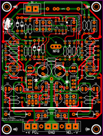
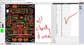
hello guys this is my final PCB prototype V1.0 and is my 5th check all components values if you guys see an errata let me know but I think is fine 🙂 I will leave the Sprint file if you want to see also please inform if any error you see to be corrected
Vargas
hello guys this is my final PCB prototype V1.0 and is my 5th check all components values if you guys see an errata let me know but I think is fine 🙂 I will leave the Sprint file if you want to see also please inform if any error you see to be corrected
Vargas
Attachments

- Home
- Amplifiers
- Solid State
- Slewmaster - CFA vs. VFA "Rumble"