
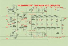
Final "Ultimate" slew output stage ....
Look over REAL good.
You , too .. Evan.
This took more time than the "old versions" .
I researched every "anal" consideration , right down to inductive X-coupling
and parasitic's.
We have ... close to the "hi-end" output stages. Should slightly outperform
1.x and 2.x , especially in the physical (thermal + power) realm.
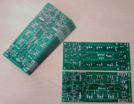
PS - will post EVERYthing later - .lay + all gerber/excellon.
This one is also intended for 2 or 3 pair builds on a 250-300mm 3U or
greater heatsink. ALL from 100W -500W can use this PCB.
OS
Look over REAL good.
You , too .. Evan.
This took more time than the "old versions" .
I researched every "anal" consideration , right down to inductive X-coupling
and parasitic's.
We have ... close to the "hi-end" output stages. Should slightly outperform
1.x and 2.x , especially in the physical (thermal + power) realm.
PS - will post EVERYthing later - .lay + all gerber/excellon.
This one is also intended for 2 or 3 pair builds on a 250-300mm 3U or
greater heatsink. ALL from 100W -500W can use this PCB.
OS
Attachments

OS, i wanted to say this since a long time: i have a lot of pain to understand what you want to say, most of the time. Be nice,can-you try to think to non native English ?
No problem , I do try to offer multiple analogies on a concept. Perhaps
more images ??
Images ,math and ,schematics are universal . Maybe "anal" (= overcompensating/overthought ) is TOO localized.
Same for many stupid acronyms .....
I'll try to keep to OPS/IPS/VAS - everyone should know those ?
Perhaps a standard acronym "sticky". I see the same ones in many threads ?
(NFB/UGF/DMM/CRO) ... and many more.
OS
Looking good. What footprint for c116 / 118? Generous enough drilling for emitter resistors? Terry and others have often helped me with boards...I hope to be able to repay the favor. You rock.....as will this version.
E
E
;-)Images ,math and ,schematics are universal . Maybe "anal" (= overcompensating/overthought ) is TOO localized.
This one i had understood. We apply the concept to sexual relationship with flies.
Look over REAL good.
You , too .. Evan.
This took more time than the "old versions" .
I researched every "anal" consideration , right down to inductive X-coupling
and parasitic's.
We have ... close to the "hi-end" output stages. Should slightly outperform
1.x and 2.x , especially in the physical (thermal + power) realm.
PS - will post EVERYthing later - .lay + all gerber/excellon.
This one is also intended for 2 or 3 pair builds on a 250-300mm 3U or
greater heatsink. ALL from 100W -500W can use this PCB.
OS
layout + all gebers etc ... oh man this is amazing 🙂 prrrrrrrrrrr 😛
Attachments

Looking good. What footprint for c116 / 118? Generous enough drilling for emitter resistors? Terry and others have often helped me with boards...I hope to be able to repay the favor. You rock.....as will this version.
E
C116/118 are 7.5mm lead spacing , 16 or 18mm. 18mm can be 680-1kuf -100v.
Mouse/newark/ digikey have these 18 x 40mm goodies in stock.
The other 4 big caps are -
C111/113 .... the driver decoupling. Up to 470uF. lower your R's to 2.2R if
you wish , this is 10X+ the size of the V1/2 caps.
C103/106 .... multiplier caps ... still 12mm (100-220uF @ 100V). Here, you
can just increase multiplier semi beta to increase filtering. A darlington
might even work here , as well .Nearly infinite virtual capacitance 😀.
All else is the same stable V1/2 layout-design - except for VFET option
pads (the "B" 's).
OS
Great job!
Looks great!
Waiting for gerbers 😉
I'm using a previous version for my current high-power build, but for the future ones - this is a real beauty - with HexFET/MT-200 compatibility - just perfect!
P.S. Huh... just imagined 5 pairs of MT-200s... Gosh... with a good PSU, one must be careful - easy to kill most of the consumer kind of speakers 😛 Concrete-crasher 😱

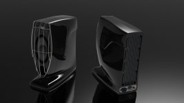
For Pete and JW and others who are helping with your contributions here I wanted to post a picture of the speaker that I intend to use these amplifiers with. I don't think I have shown it on this thread but if I have sorry for reposting it then. The height is about 16" (400mm) and is about 6" (150mm) at the widest point of the enclosure. The cone is equivalent to about a 7" speakers cone area and the dome is a 1".
Attachments
I am a bit behind you , indefixes. 😱 Very good looking - they should rock !
I sometimes do not trust my work , and triple check everything for certain standards.
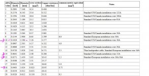
Holes -
1mm -All the big electro's , and 5W resistors.
1.4mm - output devices.
1mm - to-220/126
1.6mm - big diodes
1mm - small diodes
.7mm - small resistors
1.8mm - fastons/keystone
2.5mm - for the inductor.
1.15mm - euroterms
Some may be a little big -
2 reasons - if you need to replace anything
Some OEM's have a bigger "max" spec ,
different OEMs sometimes stray from IEC specs.
Had euroterms in the "21'st century" that I had to thin out the pins to
fit the holes., If the hole is a little large , better than a little small 🙂 .
-this has to be 100%.
OS
I sometimes do not trust my work , and triple check everything for certain standards.
Holes -
1mm -All the big electro's , and 5W resistors.
1.4mm - output devices.
1mm - to-220/126
1.6mm - big diodes
1mm - small diodes
.7mm - small resistors
1.8mm - fastons/keystone
2.5mm - for the inductor.
1.15mm - euroterms
Some may be a little big -
2 reasons - if you need to replace anything
Some OEM's have a bigger "max" spec ,
different OEMs sometimes stray from IEC specs.
Had euroterms in the "21'st century" that I had to thin out the pins to
fit the holes., If the hole is a little large , better than a little small 🙂 .
-this has to be 100%.
OS
I am a bit behind you , indefixes. 😱 Very good looking - they should rock !
I sometimes do not trust my work , and triple check everything for certain standards.
Holes -
1mm -All the big electro's , and 5W resistors.
1.4mm - output devices.
1mm - to-220/126
1.6mm - big diodes
1mm - small diodes
.7mm - small resistors
1.8mm - fastons/keystone
2.5mm - for the inductor.
1.15mm - euroterms
Some may be a little big -
2 reasons - if you need to replace anything
Some OEM's have a bigger "max" spec ,
different OEMs sometimes stray from IEC specs.
Had euroterms in the "21'st century" that I had to thin out the pins to
fit the holes., If the hole is a little large , better than a little small 🙂 .
-this has to be 100%.
OS
I think remember Jason saying his board manufacturer limits him to 4 hole sizes before charging extra. His boards had oversized pads and holes for just about everything. They are nice for reworking. Solder suckers work better with oversized holes.
For Pete and JW and others who are helping with your contributions here I wanted to post a picture of the speaker that I intend to use these amplifiers with. I don't think I have shown it on this thread but if I have sorry for reposting it then. The height is about 16" (400mm) and is about 6" (150mm) at the widest point of the enclosure. The cone is equivalent to about a 7" speakers cone area and the dome is a 1".
To not displace internal volume , the amp would need to be pretty small .
Any part of the amp inside would need to be concerned with micro-phonics and
fields from the drivers..
I'm considering this on my slew sub build. PS and caps take up < .1 ft^2 and
the port - already lost almost .3 here. But I have almost 2 cubes.
PS - my amp is almost all outside , as well. Main HS , IPS ... all with natural
convection.
An AB amp would be possible ... but an SMPS power supply looks to be
the only way. 🙁
OS
I think remember Jason saying his board manufacturer limits him to 4 hole sizes before charging extra. His boards had oversized pads and holes for just about everything. They are nice for reworking. Solder suckers work better with oversized holes.
That's a helpful hint , glad I am "pre-thinking" here.
4 sizes are no problem. 😎
OS
I agree completely about using tight hole sizes. My daughter is building one of the O2 headphone amps and put one component in the wrong position. She tried to remove the part and it broke off in the hole. She tried a solder sucker and cutting the lead off as flush as she could with the board to get it out and no way. I tried myself with a very hot iron and it is stuck big time. I am at the point that I think I am going to have to actually drill the lead out of the board, I don't see how else to clear the hole.
OS,
That is what I have been thinking that the power supply is the biggest space hog in the entire scheme of things. So a smps is more than likely the only way. Esperando is swearing by the work the Lazy Cat did that showed his amp worked best with a non regulated smps. Otherwise I have to make a third enclosure just for an external stereo amplifier. I do not want to use a chip amp, I don't think it will do the speakers justice.
That is what I have been thinking that the power supply is the biggest space hog in the entire scheme of things. So a smps is more than likely the only way. Esperando is swearing by the work the Lazy Cat did that showed his amp worked best with a non regulated smps. Otherwise I have to make a third enclosure just for an external stereo amplifier. I do not want to use a chip amp, I don't think it will do the speakers justice.
- Home
- Amplifiers
- Solid State
- Slewmaster - CFA vs. VFA "Rumble"