I like it. Why do only the NAD entries use the other half of the TL072 as a buffer and the others with a servo do not? This was evident with the earlier NAD based design.
EDIT: Duh, never mind. I answered my own question after taking a closer look.
EDIT: Duh, never mind. I answered my own question after taking a closer look.
I like it. Why do only the NAD entries use the other half of the TL072 as a buffer and the others with a servo do not? This was evident with the earlier NAD based design.
EDIT: Duh, never mind. I answered my own question after taking a closer look.
You could leave the 2'nd half idle (a grounded follower). Or you could
use the un-used op-amp as a follower (for the integrator). This is best ,as this servo is
"steering" a low Z CFB node.
It takes up to 2.5ma to zero this amp at the node , which is just seen by the
buffer. The inverting integrator itself just feeds the buffer which is
extremely high Z (80 pA load).
So , the integrator thinks it is "servo-ing" a VFA and there is no unused
op-amp. 😎
OS
Last edited:
Thank you very much jkuetemann🙂🙂
I made those changes.
Some people use other diodes series with the 15V zeners, that is OK how it is
Any other advise
Please do not worried if need some adjustment on the layout, I will do that in case if needed. That would be not a problem.
I was close to order some kits from Aussi Amplifier but with the order I must get the power supply, soft start, protection almost everything. 😱 $$$$
Yes I believe those are great kit but that just an assembly to me not really DIY.
And the pain full fact to me it cost an arm end a leg.
I'm a disabled person (due a car accident) with very little fund at the moment.
Some of the needed parts I already have like the Toshiba mosfets , transformers, PS caps etc.
So I try to full feel my dream to get the mosfet amp long time I aimed for.
Also with these a lot of option to pick the front end which feet my need, in other word I like it better.
Thank you guys one more time.
Greetings
Attachments
Make R107 the same value as the BJT version, 470R. This may need adjustment after the fact but the 100R value will give too much output idle current. That was for Hexfets.
Thank you very much jkuetemann🙂🙂
I made those changes.
Some people use other diodes series with the 15V zeners, that is OK how it is
Any other advise
Please do not worried if need some adjustment on the layout, I will do that in case if needed. That would be not a problem.
I was close to order some kits from Aussi Amplifier but with the order I must get the power supply, soft start, protection almost everything. 😱 $$$$
Yes I believe those are great kit but that just an assembly to me not really DIY.
And the pain full fact to me it cost an arm end a leg.
I'm a disabled person (due a car accident) with very little fund at the moment.
Some of the needed parts I already have like the Toshiba mosfets , transformers, PS caps etc.
So I try to full feel my dream to get the mosfet amp long time I aimed for.
Also with these a lot of option to pick the front end which feet my need, in other word I like it better.
Thank you guys one more time.
Greetings
I'm afraid that this VBE multiplier will overcompensate alot. The 1530/201 needs very little compensation is my experience: have a look at the pdf attached. This bias spreader works very good. Remark, drivers must be placed on seperate heatsinks!
http://www.diyaudio.com/forums/soli...n-subwoofer-wideband-duty-13.html#post3382545
I'm afraid that this VBE multiplier will overcompensate alot. The 1530/201 needs very little compensation is my experience: have a look at the pdf attached. This bias spreader works very good. Remark, drivers must be placed on separate heatsinks!
http://www.diyaudio.com/forums/soli...n-subwoofer-wideband-duty-13.html#post3382545
First off all thank you very much!🙂
I will take a look at your attached site, I mean I will study it, unfortunately now I have to run.
If I understood well based on your opinion it would be better to use a much simple VBE.
The driver can be placed on a separate heatsink. That is not a problem.
Also I do not need to stick with these drivers, I can use some Toshiba BJT, I got some, actually the MJE not my favorite driver al do they are acceptable work horse.😀
I can use Hitachi mosfet drivers like you I do have those in my box or I got some Toshiba matched 2SK2013/2SJ313.
If mosfet driver would be better option sound wise.
Can I come over to your thread with these amp or open a new thread...
Thanks one more time
Greetings gabor
I forget to mention I want to stick as close as possible to OS idea so I can use some of his IPS (driver stage)
I meant separate power stage and separate driver stage
A loot of great work has been done by OS! A great thanks to him!!!
Last edited:
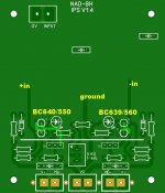
I'm back on the layout side again.
As far as either the lateral/vertical devices ... it would be good to include
zener protection across G-D. Some laterals have these internally.
I am very satisfied with my new NAD CFA.
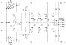
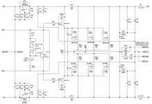
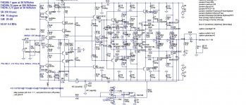
The finalized schema is (below).
I have some new component ideas (parallel CFB resistors) and
a newer more compact layout style ... 76 x 76mm is quite possible here.
-12 Q
-26 R (just 1 trimmer) no precision adjustment needed.
-14 C
-10 D
- 1 IC
- 63 parts total , not too scary (medium complexity).
The amp is the BEST 😀 in general . Best clipper , best offset , best
thermally. Also , best SLEW 😀 I did get 1K/uS with more CF applied.
All this is the direct result of the "NEW" VAS.
PS - As I said ... A CFA with VFA precision.
OS
Hi Os,
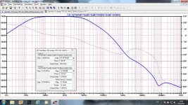
Don't take this as a criticism, I am just curious (as a cat, not lazy cat) and I simulated your NAD_BH V1.3 final as you prized it so much. I used my Vertical MOSFET OPS so there could be some differences.
First, distortion is quite high (but with good harmonic distribution), could be because od use of MIC, I am not sure and I think that with better compensation you could lower distortion even with simpler IPS. I will show that in the next post with simple VAS and with OIC.
This IPS has wery good overload (clipping) behavior, but my simulation shows marginal PM (for CFA at list), so here it is.
Damir
Attachments
Now I want to show similar amp with simple VAS, no cascode, super pairs, or EF enhanced VAS. It uses OIC compensation, ULGF is higher (but with mosfet I think is OK), distortion is quite lower, harmonic distribution is equally good as NAD_BH V1.3 and the clipping is not bad.
D. Self said that is not possible to build working amp with OIC (output inclusive compensation as per Baxandall), but I am sure it is possible with the CFA(Self does not like them). It could be very interesting if someone built it and shows that it's working.
Pity I have so many project and so little time and never built it, but it is in the line for next build.
Damir
Attachments
-
 GainWire-TIS-simple-TPC-OIC-VMOS-200W-2-DCservo-15V-betterCCS-clipping.jpg120.8 KB · Views: 269
 -
 GainWire-TIS-simple-TPC-OIC-VMOS-200W-2-DCservo-15V-betterCCS-FFT1-1W_8.jpg168.8 KB · Views: 266
 -
 GainWire-TIS-simple-TPC-OIC-VMOS-200W-2-DCservo-15V-betterCCS-FFT1-50W_8.jpg182.4 KB · Views: 278
 -
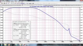
 GainWire-TIS-simple-TPC-OIC-VMOS-200W-2-DCservo-15V-betterCCS-LG.jpg306.7 KB · Views: 335
 -
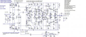
 GainWire-TIS-simple-TPC-OIC-VMOS-200W-2-DCservo-15V-betterCCS-sch.jpg159.3 KB · Views: 358
Hi Os,
Don't take this as a criticism, I am just curious (as a cat, not lazy cat) and I simulated your NAD_BH V1.3 final as you prized it so much. I used my Vertical MOSFET OPS so there could be some differences.
First, distortion is quite high (but with good harmonic distribution), could be because od use of MIC, I am not sure and I think that with better compensation you could lower distortion even with simpler IPS. I will show that in the next post with simple VAS and with OIC.
This IPS has wery good overload (clipping) behavior, but my simulation shows marginal PM (for CFA at list), so here it is.
Damir
Thanks for the 2'nd opinion on the new NAD.
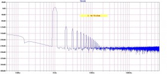
First , yes .. compared to a blameless (wolverine) , THD is a high.
Now if >20ppm (50+W) is high - shoot me !😀
1W/ 1k is .5ppm 20k = 1ppm.
I was willing to trade off 10-15ppm for the 1 cap comp. (simplicity).
Here , I was not shooting for uber low THD . I wanted the best
overall harmonic structure and overload behavior.
ALL the devices run 1.6ma , except for the final VAS cascode.
This one is made to
 SOUND the best and to be cool and
durable like a VFA.
Phase margin , a 39-47pF compensation cap value will take care of that.
This amp will simulate nice rounded squarewaves with <50PM.
And it is the BEST while running NO compensation.
BTW , your plots reflect mine nearly perfectly .... again, thanks for
a 2'nd opinion. I might try OIC !
OS
I'm interested to learn more about that quote. He really made such claim? Sorry for the OT.D. Self said that is not possible to build working amp with OIC (output inclusive compensation as per Baxandall)
I'm interested to learn more about that quote. He really made such claim? Sorry for the OT.
It started here http://www.diyaudio.com/forums/soli...-6th-edition-douglas-self-40.html#post4018122 and proceded here http://www.diyaudio.com/forums/soli...-6th-edition-douglas-self-45.html#post4019922 and here http://www.diyaudio.com/forums/soli...-6th-edition-douglas-self-46.html#post4020034 and here and next post http://www.diyaudio.com/forums/soli...-6th-edition-douglas-self-46.html#post4020034 and some posts later and finish here http://www.diyaudio.com/forums/soli...-6th-edition-douglas-self-57.html#post4030796
Thanks for the 2'nd opinion on the new NAD.
First , yes .. compared to a blameless (wolverine) , THD is a high.
Now if >20ppm (50+W) is high - shoot me !😀
1W/ 1k is .5ppm 20k = 1ppm.
OS
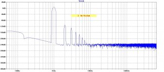
My simulation shows 4.7 ppm at 20k and 1W, 58 ppm at 50W, and 1 ppm at 1k and 1W
Damir
super VAS layout
Just a little different from the hawksford layout.
I added the super-pair current trimmer (gain). I will use BC550/640
and BC560/639 as the super-pair devices ... same BCE , KSA/C
could still be used , but are not as ideal (Vsat -Von).
The super-pair is a little "picky".
Layout has to be super tight for the Baxandall , I fear long traces would
act as a radio receiver 😀 .
This might be a "small" , very compact board. 😎
OS
Attachments
OS, you can use BC550/560 for both transistors in the super pair cascade, no need for BC639/640 not very good transistors, cascade transistor protect it from high voltage, and you can use BC550/560 for the input diamond, cheaper.
Damir
Damir
My simulation shows 4.7 ppm at 20k and 1W, 58 ppm at 50W, and 1 ppm at 1k and 1W
Damir
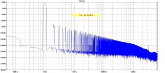
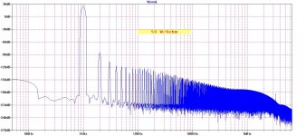
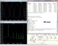
Must be your OP stage , slewmaster BJT EF3 is "cleaner".
(below) is "abuse" (3R @ >80V p-p) ... tops out at 25ppm THD20.
Bias is 77ma per device.
About 2X better than my previous versions of the nad (V1-3).
OS
Attachments
OS, you can use BC550/560 for both transistors in the super pair cascade, no need for BC639/640 not very good transistors, cascade transistor protect it from high voltage, and you can use BC550/560 for the input diamond, cheaper.
Damir
I considered that .... would still have to use KSA/C for current FB pair , they see
full rail. It's not worth cascading them.
All the others can be cheap <45v Vceo devices.
OS
Are the KSA1015 and KSC1815 OK for the lower voltage areas? Keeps the same pin out as the higher voltage devices and allows a builder to just use KSA992 KSC1845 everywhere if they so choose.
Last edited:
- Home
- Amplifiers
- Solid State
- Slewmaster - CFA vs. VFA "Rumble"