AM, on your No.3, do please take this up with McIntosh Labs. They have been at it since a wee bit before 1949...all in commercial products, and those are dealing with cathode AC voltage well over 100VAC, and heater referenced to ground.
There are, and have been for some time expensive/rare tubes that require one to 'improvise'. That the same happens with SS is of no surprise. There are very few obsolete/un-produced SS bits that are worth hunting for. A few low noise FET's and the VFET that Mr. Pass is quite fond of( the rarity or those makes NOS, United 845's look common ).
In any case AM, do please show us some of your creations, I'd like to see what your design philosophy yields( in a new thread of course).
cheers,
Douglas
On that P-Channel, source follower I can't escape the idea that a cascode would be best. Small, low voltage, low capacitance 'bottom', and TO247 on 'top' for its dissipation capability.
The benefit being a non-variable input capacitance, and thorough immunity from the negative rail I will need.
Anybody know of a battery biased, enhancement mode, P-channel PCB?
cheers,
Douglas
The benefit being a non-variable input capacitance, and thorough immunity from the negative rail I will need.
Anybody know of a battery biased, enhancement mode, P-channel PCB?
cheers,
Douglas
Hi Douglas,
that pmosfet has been used with very positive results in a PP amp (see earlier in this thread) up to IIRC 30%. Of course feel free to experiment cascoded source followers and report, I’ve never used them, but saw something by Nelson Pass about it.
that pmosfet has been used with very positive results in a PP amp (see earlier in this thread) up to IIRC 30%. Of course feel free to experiment cascoded source followers and report, I’ve never used them, but saw something by Nelson Pass about it.
To Amadeus
Totally agree with you!!
Walter
Walter,
Electronics is a science, not a popularity contest. If you have some analysis showing that the proposed circuit is unstable, please present it. So far Amadeus has failed to do so.
Each circuit I have published here is accompanied by photo of proto or final stuff with a test lab
No simulation.
Of course they can be interesting or not but this is not the problem.
If the simualtion ( after 10 pages ) remain a simulation and no proto is shown ( with preliminary test) I consider it like a smoke.
That's all.
I agree with you about electronic as a science but nobody answer me ( in the past ) in which way you can simulate a real trafo ( s.e. or pp)
Where each one is different from another with the same standard specification declared.
And I don't mean ad mid frequency where we can consider it as a ideal (less or more).
Or what I say is not real?
Note: about trafo I remeber each time this thread
OPT Characterization
Walter
Walter, in case you didn't understand the first time, here it is again:
Amadeus asserted that the circuit discussed here is unstable. You said you agree with him.
Neither one of you has provided any technical, factual support for that contention.
Amadeus asserted that the circuit discussed here is unstable. You said you agree with him.
Neither one of you has provided any technical, factual support for that contention.
This is the phrase on post 89
Simulation is all fine, unfortunately LtSpice does not model transformers too well. And the modelling is done with a pure resistance load which speakers are not.
This has all the potential of instability like the Williamson amplifier that was only marginally stable and needed a specific wound OPT.
Is "potentially", not "is unstable".
Then read post 92, please
Walter
On the reasoning one of 'em presented, I believe somebody agreed it *COULD, *POSSIBLY have characteristics that would not contribute positively towards stability. And then I recall reading that since it was developed, and offered commercially that this 'worried-about' instability has not come to light.
Now then, if youse from the moodwinite camp would please show the reason you take issue with this proven stability, I'm all eyes and ears.
cheers,
Douglas
Now then, if youse from the moodwinite camp would please show the reason you take issue with this proven stability, I'm all eyes and ears.
cheers,
Douglas
This has all the potential of instability like the Williamson amplifier that was only marginally stable and needed a specific wound OPT.
I challenge this as BS and total nonsense.
This circuit has nothing to do with Williamson and you have not shown any reason why it should be unstable. It is a SE amp with no GNFB and as such fairly low open loop gain.
If anyone has a well reasoned analysis to show why/how this circuit is unstable, please do so. There is way too much faux science going on here.

The N Fdbk thru the resistor from the plate to grid1 avoids the OT, so that seems safe as long as the Fdbk resistor is not too high in value.
The optional Fdbk from the UL tap to screen grid is positive Fdbk in the sense of a bootstrap. Any phase shift there will start to turn it into neg. Fdbk. So that seems safe, unless there is an uncontrolled resonance in the OT. A snubber across the OT primary should be able to damp that. Or just put a cap between grid2 and cathode. Can even avoid the UL tap altogether with a pull-up resistor.
We are left with capacitive Fdbk from the plate or UL tap to the MosFet gate. This would have to be at HF, so a ferrite bead or pF cap to ground there should be able to fix that. The cap from grid2 to cathode stops any HF pickup at g2. One could also put the usual RF R-L snubber, resistor with over wound turns, in the plate connection.
Using a grounded N Mosfet driver for the cathode does make good sense as far as the Mosfet goes, but Mosfet gm control turns the sound into Mosfet sound. Why bother with a tube or OT above it at all?
I suspect there will always be some SS device that can replace the P Mosfet driver in the future. The real problem is the supply of TV Sweep tubes, unless some tube manufacturer takes them up. They won't be cheap then, but they aren't cheap anymore anyway. Except for a few low performing ones.
Last edited:
S-A, I believe that changing to an N mosfet turns this into something resembling a cascode; the P flavour is just a source follower( though a fairly potent one as the cathode is a fairly heavy load compared to a grid, positive or otherwise ).
I remain convinced that the variable capacitance of the MOSFET is the reason they dono't sound like proper pentodes. Take that out of the equation( even at the expense of higher overall capacitance) seems to make them much nicer. We shall see.
I pan to use that *general topology for an open loop, zero biased triode amp, and the source follower *IS the amp I was going to have to build to drive it. Now, it is just a LTP, likely something of the vertical deflection style...which may or may not get driven balanced.
More building is good; those HY51A have been giving me the hairy eyeball since I got 'em...LOL
Oxcart of Haboo?
cheers,
Douglas
These short loops that exclude the output transformer are easy to stabilize. Nothing like the Williamson which has lots of reactive components.
My Corona SE amp is running ~35dB of feedback with no stability issues. A 2uF capacitive load provokes no bad behavior. Just normal compensation techniques were used and no expensive iron needed like in the case of the Williamson.
My Corona SE amp is running ~35dB of feedback with no stability issues. A 2uF capacitive load provokes no bad behavior. Just normal compensation techniques were used and no expensive iron needed like in the case of the Williamson.
Re: Bandersnatch
The cascode circuit will give you a pentode result. Schade Fdbk to the tube grid won't work, like it does for UnSET. Schade Fdbk to the Mosfet gate would work, but then you have the low input Z problem.
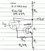
Seeing as the big TV Sweeps are nearing extinction, it would make better sense to put the N Mosfet up top for the power output. But smallish tubes can't supply the current needed for a cascode drive. I suggest trying the Kulish driver circuit below.
The voltage drop across the output device base to emitter or gate to source effectively subtracts out of the signal input, causing a distortion. The voltage drop across the power device input gets turned into a current by the resistor across it, and then gets added back into the output by the input device collector or plate.
With the bottom resistor below the output device set to near the same resistance, this current is similar to what would have been demanded if the device did not have the Vdrop. So the output device's finite gm effects can be tuned out.
With a triode for the input device, the plate provides Voltage N Fdbk as well, turning the whole combo into a power triode (with fairly limited current variation thru the input triode). So you just need to find an input tube with good triode characteristics.
The cascode circuit will give you a pentode result. Schade Fdbk to the tube grid won't work, like it does for UnSET. Schade Fdbk to the Mosfet gate would work, but then you have the low input Z problem.
Seeing as the big TV Sweeps are nearing extinction, it would make better sense to put the N Mosfet up top for the power output. But smallish tubes can't supply the current needed for a cascode drive. I suggest trying the Kulish driver circuit below.
The voltage drop across the output device base to emitter or gate to source effectively subtracts out of the signal input, causing a distortion. The voltage drop across the power device input gets turned into a current by the resistor across it, and then gets added back into the output by the input device collector or plate.
With the bottom resistor below the output device set to near the same resistance, this current is similar to what would have been demanded if the device did not have the Vdrop. So the output device's finite gm effects can be tuned out.
With a triode for the input device, the plate provides Voltage N Fdbk as well, turning the whole combo into a power triode (with fairly limited current variation thru the input triode). So you just need to find an input tube with good triode characteristics.
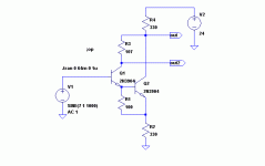
Attachments
Last edited:
SA, what I have in mind is to just drive the cathode of the HY51A. The power triode is a very fine one, and its curves are nearly perfectly balanced across a +/- 30V swing around 0V and plate resistance is not too high. The source follower built around a P-channel MOSFET did not occur to me before...LOL
I don't want any of the stages dealing with grid input resistance discontinuities, and NFB is not needed save perhaps to lower output Z...and since this will drive a horn-loaded transducer, that is no issue either. Nor is its overall power output( though I expect near 50W from it ). So...tie grid to ground, build a negative rail of ~60V, of power handling capacity, and then drive a resistance coupled gate and we're off to the races with a missing tube power stage, and no IT.
Aside from the source follower implementation, it is a bit off the thread topic... 🙂
cheers,
Douglas
Each circuit I have published here is accompanied by photo of proto or final stuff with a test lab
No simulation.
Of course they can be interesting or not but this is not the problem.
If the simualtion ( after 10 pages ) remain a simulation and no proto is shown ( with preliminary test) I consider it like a smoke.
Walter
I spent much of my engineering career at Motorola turning the stuff that the simulation and calculation boys did on paper (or presented in Powerpoint) into real prototypes of two-way radios, sub-circuits or or other real touchable, measurable, useful quantifiable devices. After all Motorola sells two-way radios, not slick Powerpoint presentations.
Mu Tubelab stuff is done much the same way. I use LTSpice to find out what will not work, find weaknesses in a working design, or just to try out some of my DUMM ideas. The UNSET actually began as a 6KD6 on a test board with a pair of mosfets on each grid and the cathode. I had two phase drive with the ability to sink or source current into each element. I spent nearly a year tweaking on this before I ever put anything into the simulator.
Anything I post on diyAudio has been built and tested unless I state otherwise.
Once I had several working sims, I actually built a push pull board and a couple SE boards. They were thoroughly tested, then connected up to speakers and a CD player. One of those test boards was my main listening amp for over a year, so this design IS very real.
The test data including the usual frequency response, THD VS power output, and THD VS frequency data in in post #43 here:
UNSET is coming?
I posted my simulation in that thread so that others can play with it. If Zintolo and others want to simulate stuff for years or twist the design into something new, that's their choice, and I have no problem with that. Simulations however, are rather boring to listen to, and at some point it would be good to actually build something.
The schematic of the final board is in post #236. As stated in that thread, the parallel mosfets are not real, only a single mosfet is used in the board at a time. The fets can be placed on the top or bottom of the board, so two are shown on the board layout schematic, along with a lot of holes.
Their isn't any resistor discontinuity with the Kulish circuit, that resistor would normally be there for a pull-down anyway, it's just boot-strapped in the Kulish design. (for the bipolar transistor case, 0.6V across it just looks like a CCS) Input to the circuit is still high Z.
The Kulish driver, with a tube input, does require sufficient voltage across the input triode to function, unless a floating supply is provided for it.
With a floating supply included for the input triode, the Mosfet can operate with minimal voltages across it. Maybe allowing the OT to be left out.
The Kulish driver, with a tube input, does require sufficient voltage across the input triode to function, unless a floating supply is provided for it.
With a floating supply included for the input triode, the Mosfet can operate with minimal voltages across it. Maybe allowing the OT to be left out.
Last edited:
SA, the '51A will be zero biased...and therefore an increasing signal will work into a current sponge grid, while a negative one won't. That is the beast of the design as presented for subscript 1 operation; grid current gives the FB resistors fits. Not criticism, just not OK for me who is going to deliberately twist this into something else entirely 'cause I have the bling-ey TT cathode power triodes to apply it to.
Now applying this FB circuit to something really bonkers like a pair of GU-81m is not without its charm. Probably best to try Class A 813 first if I can find an OPT...LOL
Rock On there Tubelab.
cheers,
Douglas
Now applying this FB circuit to something really bonkers like a pair of GU-81m is not without its charm. Probably best to try Class A 813 first if I can find an OPT...LOL
Rock On there Tubelab.
cheers,
Douglas
- Home
- Amplifiers
- Tubes / Valves
- Single Ended: the pentode retaliation