My experience is also: 8x OS with stopped clock was significantly better sounding thank 4x. Albeit with different DFs. Without slew limiting but with limited HIGH voltage (I used 2V logic ICs for the last stage).
Did you compare stopped clock vs. continued clock at the same FS? How would you describe the difference in sound quality?
Did you compare stopped clock vs. continued clock at the same FS? How would you describe the difference in sound quality?
My experience is also: 8x OS with stopped clock was significantly better sounding thank 4x. Albeit with different DFs. Without slew limiting but with limited HIGH voltage (I used 2V logic ICs for the last stage).
Slew rate limiting is the critical part. Which you did not do.
How you can even do 8 X OS with stopped clock on the TDA1541 is a marvel in itself.
Did you measure the system actually did perform as expected and that the clocks etc. were what you expected? Anyway, I'm uninterested in oversampling.
Thor
Ok, I asked 2 times if you tested the sound quality. You didn't answer. I did tests. I know how it sounds. Zoran as well. So please be a bit more polite and do your homework instead of repeating "suit yourself".
I know how it sounds.
But you do not know what a slow continuous clock with slew rate limiters sounds like. Do you?
I know what minimising the BCK feedthrough overall measures and sounds like. And I know what stopped clock looks like, at the analogue output.
do your homework instead of repeating "suit yourself".
I'm afraid you will hear it again.
I have my objectives. You have yours. There is almost no overlap.
I am not interested working to create something I explicitly do not want.
After seeing what real interest is there in what interested me, seeing nobody is interested to work jointly.
I will do whatever I have to for my use. And it will be closed source, naturally. That's fine.
So if you want what you want, you must suit yourself.
Thor
Last edited:
I would but my knowledge of digital donain is quite limited. What i can do is offer my time in pcb design.After seeing what real interest is there in what interested me, seeing nobody is interested to work jointly.
I will do whatever I have to for my use. And it will be closed source, naturally. That's fine.
Would like for this topic to progress, so it would be nice to remain limited to the op requirements.

I know what minimising the BCK feedthrough overall measures and sounds like. And I know what stopped clock looks like, at the analogue output.
Thor
Why don't you show these people what stop clock looks like at the output in a build made by YOU , you'll gain in credibility in this matter
after all , if stop clock is the wrong way it will be easy to show it off with nice own measurements
.
@ThorstenL
Hi Thorsten, I do appreciate your knowledge and trying to help out with this DIY project! I am still waiting for a PCB/motherboard to use with the TDA1541A chips I had ordered at a fairly high price. I do know that Brijac is an ace with designing PCB's! If he is willing to put in the time for designing a PCB, that would be great! We know you have great knowledge about this project, so please keep up the good work! 🙂 Just my 2 cents! Have a nice day 🙂
Hi Thorsten, I do appreciate your knowledge and trying to help out with this DIY project! I am still waiting for a PCB/motherboard to use with the TDA1541A chips I had ordered at a fairly high price. I do know that Brijac is an ace with designing PCB's! If he is willing to put in the time for designing a PCB, that would be great! We know you have great knowledge about this project, so please keep up the good work! 🙂 Just my 2 cents! Have a nice day 🙂
Would like for this topic to progress
Well, what I would need most in terms of contributors is someone with a working digital sim that includes the 40105 FIFO in the library to validate the design. Spinning new PCB's get's expensive so one would probably want to start with a working design.
The second part would be to work on PCB's, here multiple pairs of eyes will catch mistakes a single pair doesn't catch, again because printing PCB's has minimum order levels and it gets expensive to get it wrong.
Conceptually it's easy enough.
We want to extract two parallel 16-Bit Data streams from standard IIS with 64 Bitclock cycles per sample and invert MSB.
We want to output this data as TDA1541 SIM datastream with LE pulse and 16 Bitclock cycles per sample.
We also want a fixed DEEM Clock synchronised to MCK at 8 X 44.1/48kHz.
There are a few angles we can take to do this.
As mentioned, if we have two independent FIFO's at least 32 Bit long (e.g. 74ACT2226 etc) it is the most easy way to do. But these IC's are like hen's teeth.
We need a 32 bit FIFO so we have 16 Bit we clock out. The last input bit from IIS will arrive when we are clocking out Bit 4, not enough to make do with 16 Bit only.
It would also work this way with 4 X 40105 to make two 32 Bit FIFO's with independent clocks. Less than 32 Bit will not work.
Or we use 2 X 40105 as 4 X 32 FIFO and pass LE, DATA-L, DATA-R through this. But we now need a 32 Bit delay/storage to align things on the input side. So we don't do much better on IC's.
Gate the input clock to only allow a bit to be input when the correct bit is present on the input, invert MSB. The bit ripples to the "top of the stack".
On the output simply clock out out bits once the half full flag is raised. We will have have 16 Bit (or more) in the FIFO and we will get 16 bit's into the FIFO for each WCK period.
Add reclocking and signal conditioning as desired.
Done.
Of course, we can also do it using a 64 Bit Shift register chain ( 8 X 74xxx595) to hold the full data word and two 16 Bit Shift registers (4 X 74xxx165) to pick up one sample and output in parallel.
That's probably 16+ IC's once we are finished.
Or we accept a higher BCK frequency and just cheat.
Thor
Last edited:
Before recklocking dugutal isolation?Add reclocking and signal conditioning as desired.
Recklocking with 2 x F-F serial searate for each line.
.
With separate PS and isolation at Analog out that will be completed DA isolated unit.
Before recklocking dugutal isolation?
Isolation is best placed as far backwards as possible. But it is not necessary in any any sense, correct design and layout can remove the need for isolation. All commercially available digital isolators are horribly high jitter.
Recklocking with 2 x F-F serial searate for each line.
Why? This is only necessary if crossing multiple clock domains where the clocks are of the same frequency but with a unpredictable phase/delay response.
Then the input flip flop needs to clock on the highest available clock from the source or 2 x BCK as minimum and the output flip flop with the final clock.
With separate PS and isolation at Analog out that will be completed DA isolated unit.
Much more mileage in actually dealing with the problems the TDA1541 has build in. In competent designs isolation is not needed, useful or beneficial, rather it creates a multitude of problems to solve.
Seems like a great idea, but it's not.
Easiest solution to isolation. Use SPDIF and a separate system clock. Use Gigabit LAN isolation transformers (< -1dB @ 100MHz if correctly terminated).
Which brings me back to the CS8416...
The WM8804/05 was good enough on jitter in practice to equal most "Femto clocks" but is EOL. With the 880x you can ditch the second clock.
The final generation of AMR CD-77 had USB in via XMOS and SPDIF via 8805, together with the redesigned TDA1541 PCB. Results were excellent, but problems with supplies of the casework meant production was paused and never resumed.
Thor
Well, what I would need most in terms of contributors is someone with a working digital sim that includes the 40105 FIFO in the library to validate the design. Spinning new PCB's get's expensive so one would probably want to start with a working design.
The second part would be to work on PCB's, here multiple pairs of eyes will catch mistakes a single pair doesn't catch, again because printing PCB's has minimum order levels and it gets expensive to get it wrong.
Conceptually it's easy enough.
Thor
If it's that easy , why dont you do it ? , if I had the knowledge you say you have , it will be allready done 😉
.
Try Labcenter Proteus.working digital sim that includes the 40105 FIFO in the library
Try Labcenter Proteus.
Will have a look.
Meanwhile I remembered the old TI SRC4190 as format converter and (optional) dejitter (and Digital Filter). It retains active status at TI and is good supply at mouser.
We can operate the output as slave with a BCK of 32 FS. Now we have a 32 FS IIS out from either CS8416/DP7416 or an Amanero. It was used like this in the AMR CD-77. So i know it works and sounds ok. 6.74 USD is still a bit dear.
All of this in principle gets us back to a minor variation of the CD-77 MKIII (unreleased), which was designed with much less understanding. Interesting.
Thor
All of this in principle gets us back to a minor variation of the CD-77 MKIII (unreleased), which was designed with much less understanding. Interesting.
An alternative would be to use a delay line with 32 Bit and to delay WCK by 1 BCK like so:
Use a 1-Shot that generates a 1 BCK wide LE pulse suitably aligned to go into the FIFO with our data. This LE pulse also triggers the MSB inversion before the FIFO (or after, if we must).
The best we can do for a 16 Bit SR with 32 Bit delay is 1pcs of 74xxx16374 to hold 16 Bit (stopped clock on the 16 Bit load).
The clock logic will be interesting.
Using 2pcs for a 32 Bit delay simplifies logic, but uses one more big chip. The complete stopped clock logic goes back to AN-207 from AD:
Either way, we use stopped clock on the inputs
Instead of the DAC's we have a Delay in one channel. 32 Bit delay (for 64 X FS IIS) or 16 Bit delay and 4 Bit counter for clock control. Not really a material difference.
But we need the 16 Bit counter anyway to gate off the input clock of the FIFO. A 32 Bit counter actually.
So we use a 74VHC393 as 2 X 16 Bit counter (so technically it will count to 256, we just take the top 5 bits). We can also get BCK/4 from this counter to send downstream.
Add 74LVC16374 as 16-Bit SR and 74LVC74 etc. and a few gates, voila we are good on the input logic.
We can now enter 2 channels of DATA and the LE pulse into a 32-Bit FIFO made from 2pcs 74HC40105. Output clock is continuous input BCK / 4
We re-clock the BCK on the output, as well as DATA-L, DATA-R and LE with MCK. Use any of the 1G79 options in SC-70 that have decent timing and jitter at 1.8V, preference to SN74AUC1G79DCK but others exist.
This will take any IIS 4-Wire source (with MCK) and output Simultaneous conditioned to the TDA1541 input with 1.8V Peak-Peak swing.
If we use a large value series resistor directly at the TDA1541 input and let internal capacitance to -15V handle the slew rate limiting or if we put external limiters are a matter of debate. If we put an RC next to each SN74AUC1G79DCK all currents circularise there, but are much larger. The actual current through the 12pF base capacitance to substrate in the TDA1541 substrate is the SAME, no matter if you just a series resistor or an external RC, as long as the rise time/slew rate is the same.
So my take is that it is better to use a large value series resistor directly at the TDA1541 as this keeps all circulating currents to the minimum.
We have a maximum BCK of 3.072MHz at 192kHz, so the narrowest BCK pulse width is 162nS. A rise (and fall) time of ~40nS should be sufficient. Now 40nS & 12pF suggest a 3.3k resistor directly at the TDA1541 Pin's and a 50 Ohm transmission line (Cable/Stripline) from the reclocker, which being AUC is 50 Ohm Zout to match a transmission line
Does anyone see any logical flaws here?
Thor
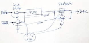
With 3state gates you could solve the input selector and a final reclocking stage:
I could. I tend to use something 74xxx16244 as selector for multiple I2S inputs in commercial designs, using the OE pins. It makes a nice layout as result of the flow through design and decoupling arrangements are good due a sensible pinout.
I would avoid this for the master clock.
In some of the lower end stuff I use NC7SZ157 as clock selector. Higher end gear uses relays.
I am very much trying to avoid using anything that needs code, if possible. This is DIY. I don't want to do what I would for work.
Anyway, sorting this out is the least of the problems here.
Thor
Exactly: hence my proposed solution doesn't even need a clock selector.
I get that.
But is that particularly relevant to the management of the Dataflow into the FIFO? This is the interesting part and the one where I need a logic sim.
Thankfully anything but the FIFO is in the Tina library, so I can re-use existing sim's to a degree. Now I need to find the Parsley, Sage, Rosemarin and Time...
Thor
the management of the Dataflow into the FIFO?
Ok, I put on the Captain Morgan cap and went outside under palms and had something very cold from a very big sweaty glass. Watching cats, birds etc.
I figured we can use a 40105 FIFO for the 16 Bit delay and it gives us most of the flow control.
Our first stop, we delay WCK and align the falling WCK edge with the falling BCK edge.
Now, while WCK is low we enter bit's into one lane of a 40105, I call that FIFO0.
Once the first 16 MSB are in the FIFO we can keep the clock going, the FIFO will just ignore the extra bits, as we are not clocking out. We now have 16 Bit in the FIFO ready to go, but no clock on the output.
When WCK goes high we enable the output clock on the FIFO and keep the original data going.
We now have the 16 MSB of the DataStream L/R and we clock these into the next 40105, I call that one FIFO1.
By using FIFO0's DIR Flag and delayed WCK with an EXOR gate we can make the 1BCK wide LE pulse that also enters FIFO1/2. And we can use this pulse to invert the MSB's while they enter FIFO1 using another two XOR gates.
When FIFO0 hit's empty we stop the SI clock to FIFO1. The 16 bit's we entered into the FIFO1 have rippled as far right as possible, we have 16+n (where n is likely 4) bit's in the 32 Bit FIFO made up from FIFO1 & FIFO2.
We have a continuous clock of BCK/4 running on the output of FIFO2. So for every WCK period we clock out 16 Bits. The data in the FIFO varies between 8 Bit's (shortest) and 20 Bit's.
So here the full timing diagram. I think the logic that remains to solve is trivial.
We need 3pcs 74HC40105, 1pc 74HC86, some flip-flops to divide BCK & MCK and our output reclocker latches. Some more gates to handle clock gates.
And we get a nice buffered stream at BCK IIS / 4.
Again, anyone see any mistakes in the timing diagram?
Thor
- Home
- Source & Line
- Digital Source
- Simultaneous output Frontend for TDA1541 (and or Universal Multibit DAC) using discrete logic - Collaborators wanted