It looks like Japanese OEM. Maybe an old Nagaoka? Someone will spot it. In any case, soon enough, Kent will finalize the PCB for phono & Shunt for standard parts designations. It will be cascode first stage, so self capacitance will be negligible and there will be a Cx load capacitor position for adding the capacitance needed for any cart above the capacitance of cabling. So cable capacitance + Cx = total capacitance specified. There will be one common board for the phono and one common board for the 3 different voltage but same schematic improved shunts. Out of 3 respective schematics with same part names but different values and PSU voltage you will be able to construct either MM, high MC or MC. You can make the MM version then.
RCruz said:Thank you Salas
...
It is good to know it affects the lower freq 😀 (I would love to see a plot of the two situations)
Ricardo
Don't try to use it as EQ for bass, because beyond some slight tailoring of the total trend, stronger RIAA manipulation is surprisingly audible all over the tonal character in my experience. It probably has to do with the total transfer function and has impulse / time domain implications.
Russian 47nF cap size
Hi Ricardo (or anybody else)-
When you get the 47nF caps, could you post dimensions? I would like to allow for larger (within reason) components on the PCB.
Thnx- Kent
RCruz said:
The bulk is the problem in this case. They did not arrive yet so I do not know the exact size. Maybe I can fix them under the pcb.
Ricardo
Hi Ricardo (or anybody else)-
When you get the 47nF caps, could you post dimensions? I would like to allow for larger (within reason) components on the PCB.
Thnx- Kent
Re: Russian 47nF cap size
Ricardo
I will, as soon as I get them.kstlfido said:
Hi Ricardo (or anybody else)-
When you get the 47nF caps, could you post dimensions? I would like to allow for larger (within reason) components on the PCB.
Thnx- Kent
Ricardo
salas said:
Don't try to use it as EQ for bass, because beyond some slight tailoring of the total trend, stronger RIAA manipulation is surprisingly audible all over the tonal character in my experience. It probably has to do with the total transfer function and has impulse / time domain implications.
I was afraid it would me more complicated than I initially believed.
So 47nF should be the final target.
PS:
Yesterday I turned the Riaa on after beeing listening for the CDP for three days (These two modded items share the same input in the 101 so I must redo the cabling connections everytime I want to change source
 ) .... What a difference !!!, the treble information is so much more vast and coherent and the bass is now very tight and controlled. (I did some more adjustments in the sub and added some weight to the headshell
 )
)As is the Riaa is superlative.... never had any source sounding so good before....
I am reporting this because now some of you might be having doubts about using a PIO for C2 47nF on the Riaa circuit.... It works like wonder

My intention to replace this cap with a clearer one is now merely academic... I want to know the differences.. (In my CDP DOS I am using only polystyrenes and the sound is quite sweet with very tight and controled bass).
The DOS is a discrete output stage "PWM passive filter + jfet diff amp + jfet output buffer" so the circuit is quite similar to the Riaa.
Hope I am not beeing over boring.. just learning😉
Ricardo, you're not boring me, that's for sure. As a novice to such fine tuning I find this very interesting. So, thank you!
I am enjoying this phono stage every day and like it very much. Sadly the power amp + speakers lag miles behind the headphone amp + headphones, so it's a one person at a time listening when good quality is desired.
I am enjoying this phono stage every day and like it very much. Sadly the power amp + speakers lag miles behind the headphone amp + headphones, so it's a one person at a time listening when good quality is desired.
salas, something that might be interesting to you and anybody else that is using your regulator.
http://www.diyaudio.com/forums/showthread.php?postid=1780592#post1780592
Something I have omitted to say in that post is that the variation of your shunt regulator that I am using measures just a little more noise than the noise of the quietest LED I have. I guess I'm saying this as another confirmation that your regulator is performing very well
Thanks Iko for the noise tests. They confirm what jwb said also. Its noise, at limit down. Most important thing for me in a reg for MC Riaa. Mission accomplished as they say.
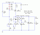
The local CCS currents have shown smoother overshoot with some damping. That helped the overall step test transient behavior.
See test
In the resume posts to come with Kent's Riaa and reg PCBs, the reg will have the R6 mod as standard, and will be Vbe CCS. Enhanced with local JFET as it happens with the LEDS example. So no fine tuning of R1 regarding to various LEDs. Vbe is standard for silicone. That will be the finely tuned and noise/output impedance tested reg recommendation with its mate PCB, as Ikoflexer have looked into the finer details of its circuit performance, and will assist Kent with the layout points of attention.
Please remenber that the placement of the mosfets is critical... need some distancing so these can be easily heatsinked 😉
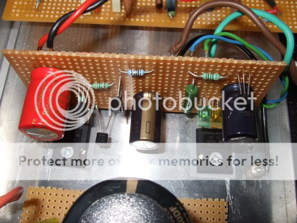
Riaa proto
From now on, and contributing for my peace of mind, I will consider my Riaa as a prototype.
After my last modd (FT-3 on the Riaa) and replacing the second jfet on the Riaa (Q2), I believed I solved the noises issue.... Yesterday I decided to power off the Riaa during dinner and when we came on at night, it took 1 hour to stabilize... thunder, spitting and other noises reappeared on the left channel.
In the past I replaced Q3 and Q5 without improvements... So I believe my method of search and destroy is no good.
The next one will be built from scratch with new jfets and a new board from Kent.
Hi Kent
In order to enable us "supernoob padlifters" to replace some components and fine tune without destroying the pcb, it should have large solder pads for C4 (output), C1 C2 C3 (Riaa) and Rx (Cart Load).
Also, would you please verify if we can use 16mm diameter caps for C10 and C5 (+V decoupling)... It would be great to use 680uF 35V BGNx there.
PS:
Depending on the thickness of the copper we use in the pcb, things might get a little nasty (resoldering wise) so I believe large tracks are a must.
Regards
Ricardo
Ricardo, if I may suggest an alternative which is highly superiour for trying things out to a PCB. It is a combination of point-to-point and PCB. The idea is to create a small PCB island for each spot in the circuit where more components get together. You start with a double layer copper board. One side will be B+, the other side will be the ground plane. Yes, you get a real ground plane 🙂 Then from another double layer copper board you cut a strip 5 to 10mm wide. Out of this strip you will cut the "islands" or pads, each as long as you think you need so that the components will be soldered onto them. Each pad is soldered onto the ground plane on one side, and the other side is used for the components pins. For the occasional B+ connection in the middle of the board you can put a small hole to pass a wire to the other side of the board, where B+ is.
This method has a lot of advantages, including immediate access to ground, ease of re-soldering and moving things around, good HF properties with the ground plane on one side, and the B+ on the other.
This method has a lot of advantages, including immediate access to ground, ease of re-soldering and moving things around, good HF properties with the ground plane on one side, and the B+ on the other.
hum ,there is a lot paper on pcb ground problem and so on...soldering on big ground plane is a problem too
use pre hole pcb as Salas and use P2P to joint ....I know that dont look good but work and sound well ,remember pcb is a caps ....
use pre hole pcb as Salas and use P2P to joint ....I know that dont look good but work and sound well ,remember pcb is a caps ....
ikoflexer said:Ricardo, if I may suggest an alternative which is highly superiour for trying things out to a PCB. It is a combination of point-to-point and PCB. The idea is to create a small PCB island for each spot in the circuit where more components get together. You start with a double layer copper board. One side will be B+, the other side will be the ground plane. Yes, you get a real ground plane 🙂 Then from another double layer copper board you cut a strip 5 to 10mm wide. Out of this strip you will cut the "islands" or pads, each as long as you think you need so that the components will be soldered onto them. Each pad is soldered onto the ground plane on one side, and the other side is used for the components pins. For the occasional B+ connection in the middle of the board you can put a small hole to pass a wire to the other side of the board, where B+ is.
This method has a lot of advantages, including immediate access to ground, ease of re-soldering and moving things around, good HF properties with the ground plane on one side, and the B+ on the other.
Hi ikoflexer
this is a wonderfull idea. Somehow it makes me think of the 101b layout: A base pcb where you connect the heavy stuff (PSU + connectors) and several smaller pcb (I have three) connected to the main board by gold pins.
Very easy to mod.
But in this case, I would need much help to design all those small pcb.
Maybe "full on" ptp is the way to go for me.
As I am new to this, would you please send me a link with a good perforated board ?
Ricardo
- Home
- Source & Line
- Analogue Source
- Simplistic NJFET RIAA