If I opted by using two parallel devices on the input I know I will dramatically reduce noise but what happens with input capacitance ? Does it go up a lot ? Does that influence bandwith reducing it ?
3dB better noise is not dramatic if its already adequate for your cart. Capacitance goes more of course. Good thing is that THD is not affected much due to very low swing there anyway.
I read that "Linearity does not nessecerely improve, but you might end up with less low order, and more high order distortion."
Do you agree with this quote ?
PS: You have mail 🙂
Do you agree with this quote ?
PS: You have mail 🙂
Submarines, watch out.
Glup !
What a size 🙂
In real world are bigger than in a photo🙂
Well better luck on v1.2 tomorrow. 1 brd won't light the LED. have 0.625V at load. Q4 stays stone cold but Q1 generates a small amount of heat. Need to make sure I have d1 in correctly.
The second brd lets the magic smoke out of R1. (Instantly) Need to pull the caps off and get out my 3x reading glasses and get personal with the board. Obviously I have a whisker somewhere or a cold joint.
Don't worry I suffer the same several things (last was a break joint joint in the reg) I wish you good lucky next time.
Let us know your subjective opinion usin dual Tx & regs?
3 dB, as Salas pointed out. Unless yoy would like to "copy" Accupahse in its lastest C27 phono stage (>10.000 €) where is using 16 (sixteen!) BJTs in parallel to further reduce noise (well, actually 32, as it's a symmetric topology) 😉If I opted by using two parallel devices on the input I know I will dramatically reduce noise....
Hi Massimo
I also read that "Noise will go down with the square root of parallel devices"
If that is right, than Accuphase must really be silent (depending on what type of BJT it is using) 🙂
I also read that "Noise will go down with the square root of parallel devices"
If that is right, than Accuphase must really be silent (depending on what type of BJT it is using) 🙂
The old but always good 2SC2547 & 2SA1085 in the front end (powered by the simplest shunt reg: resistor + zener 😉 )
Quick Update. Found that Q1 was blown on second board. (replaced). I also verified that LED is installed correctly. Have not retested yet and will do this weekend, after rechecking all joints. I also want to reverify that BJT/jfet orientations are correct(again).
3 dB, as Salas pointed out. Unless yoy would like to "copy" Accupahse in its lastest C27 phono stage (>10.000 €) where is using 16 (sixteen!) BJTs in parallel to further reduce noise (well, actually 32, as it's a symmetric topology) 😉
I'm not going balanced to have more gain😉, I'm going balanced to avoid ground loops🙂 & avoid esoterics wires😀.
I will use only five 2SK170BL per four channels = 20 pcs (1st stage 2 parallel & 2nd stage 2 parallel & the other one with LEDs string) as Salas suggested by pm, the great new is that with the new schematic only will need 2.2uF like output cap🙂
Also I have in mind to make 4 regs V1.2 one for each channel, of course 4 Tx one for each channel.
I read that "Linearity does not nessecerely improve, but you might end up with less low order, and more high order distortion."
Do you agree with this quote ?
For what you read that? Cascode, or paralleling? This phono shows more 2ndH than 3rd as a whole in all configurations measured till now BTW.
Quick Update. Found that Q1 was blown on second board. (replaced). I also verified that LED is installed correctly. Have not retested yet and will do this weekend, after rechecking all joints. I also want to reverify that BJT/jfet orientations are correct(again).
Mostly orientations tend to got wrong, or some joint missing, check those well.
How about substituting a 2N5459 for Q6? Somehow during the pcb design I did that. Should be a 2N5457. Doesn't explain why the LED doesn't light up however.
Can change the OLG and upset compensation. 2N5457 or BF245A. Trim down the 5459 to 2.5mA with a resistor between S and its now connection point is a fast test. Are the BJTs correctly oriented, those cascoded above the LED and the Mosfet controlling BJT too? Burning the CCS Mosfet or R1 smells its not controlled.
P.S. I have had some Riaa curves still in the FFT memory banks and centered them like in the Ref Spice graph. They fall so near, and frequency bins undulations or any card correction file and visual precision makes it hard to know if its dead on or just very slightly off. It falls in measurement system calibration and subjective territory given the cart and rest of system to play with C3 or not. Its our LCR DVMs that can play, everything. But I would not tune heavier than 100-150pF tolerance subjectively.
P.S. I have had some Riaa curves still in the FFT memory banks and centered them like in the Ref Spice graph. They fall so near, and frequency bins undulations or any card correction file and visual precision makes it hard to know if its dead on or just very slightly off. It falls in measurement system calibration and subjective territory given the cart and rest of system to play with C3 or not. Its our LCR DVMs that can play, everything. But I would not tune heavier than 100-150pF tolerance subjectively.
Orientation looks correct on Q9, Q2, and Q8. I did find an ultimate oops. During the build I found a tube with matched IRFP9240 written on them. Had a sticker with respective Vgs on the front from the excersize several years ago. So I used them.
Got curious a few minutes ago and pulled the sticker off to reveal that they are IRFP244's. I have now replaced them with IRFP9140's and will take a few minutes off to pick-up my kids from football practice and regain my pride.
Must remind myself that ASSUME is an acronym.!
Got curious a few minutes ago and pulled the sticker off to reveal that they are IRFP244's. I have now replaced them with IRFP9140's and will take a few minutes off to pick-up my kids from football practice and regain my pride.
Must remind myself that ASSUME is an acronym.!
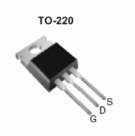
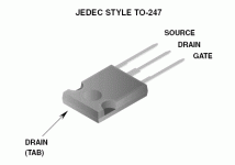
Pleas confirm the following. On the IRF9610 and IRFP9240, the pinout is as follows.
Looking at the device from the front, pins 1, 2, 3 from left to right. Pin 1 = Gate, Pin 2 = Drain, Pin 3 = Source.
Is that correct. I have verified the rest of the BJT's and JFets to be correct.
What I have now is no current passing what so ever. LED is out. Drain on Q1 is at 0V while S is at 60V. Gate is 0.15V. E and B of Q7 are at 60V while C is at 0.15V,
That is way above the max allowable Vgs for Q1 so I will assume it is blown. Q7 is probably also toast as it has a Vce of 45V
Last edited:
Assuming your connections and orientations are OK, some things may have blown in your previous NMos power up. I would change the error amp BJT and 2SK170 first. Mosfets don't blow up in that circuit so easily. But in such a scenario you may have well given it a general haircut. The LED would need some Vin-Vout to come up. Well above 0 Vo. Also did you start your trimmer half way? Are the sense and force all connected across the dummy?
Attachments
- Home
- Source & Line
- Analogue Source
- Simplistic NJFET RIAA