hey Ruwe,
if im reading it right you have the vbe transistor mounted "on top of" one of the output trans?
if your mounting goes; heat sink, output trans, vbe trans, in a stack, then the vbe will only pick up and bias that output side and not both, this is probably the reason you get a swing to rail voltage, its the other side thats running away.
standard practice is to mount the vbe equal distance in between the output devices and directly on the heat sink. this should solve some of your problems with current stability as well.
hope it helps, steve.
Excellent deduction Steve, one does not always think about how the Vbe multiplier is mounted and what effect it has.
Member
Joined 2009
Paid Member
interesting - I've never seen this happen in my other amplifiers - Vbe mounted on one device has always been sufficient. If one output only has run away and the output has gone to the rail, doesn't the -ve feedback loop compensate for the dc-offset and pull it back ?
Yes it will eventually compensate - but I think what Steve says and it makes sense, is that the Vbe multiplier will respond almost instantaneously to the transistor it is mounted on, giving quick fluctuations, while mounted on the heat sink will be gradual due to the thermal lag.
Member
Joined 2009
Paid Member
The other problem with my version is the current adjustment, i.e. the Vbe multiplier. The current is unstable and I saw on several occasions the transistors going slowly in thermal runaway in idle (and, yes, my heatsink is big). On the other hand the circuit is somewhat underbiased. The current may stabilise at say 150mA, but if you run the amp for few minutes with 100Hz sine wave at about 5W of output power, the current will drop and you'll see classic crossover distortions on the output signal. The Vbe multiplier transistor is mounted on top of one of the output BJTs.
1. How can I limit the bandwidth to something more normal, like 5-500kHz/3db? 🙂
2. How can I make the feedback to work only from 2-3Hz and above, this way expecting more stable DC offset?
3. How can I stabilize the idle current adjustment and make it less "touchy" and less temperature sensitive?
4. How can I safely turn on this thing without readjusting it every time? ... Without DC servo if possible
Regards to all and special thanks to Lazy Cat for the ingenious circuit.
In my simulations I see sensitivity to temperature of not just the input devices (can affect VAS current as well as dc-offset) but also to the temperature of the VAS devices. I'm wondering if you have one VAS device warming up a bit slower than the other ? - if one VAS device is turning on a bit slower the dc-offset will shift during start up until the amp reaches the temperature that it was at when you set the dc-offset to zero.
To make the feedback work only at a.c. you have to put a capacitor in series with the feedback shunt resistors - a common practice on many of the amplifiers you can find on this forum - such as the JLH 10W Class A.
I am currently working through the temperature stability issues myself - you can find my thoughts here: http://www.diyaudio.com/forums/solid-state/196973-tgm5-all-bjt-simple-symmetric-amplifier.html
Yes it will eventually compensate - but I think what Steve says and it makes sense, is that the Vbe multiplier will respond almost instantaneously to the transistor it is mounted on, giving quick fluctuations, while mounted on the heat sink will be gradual due to the thermal lag.
I agree it will respond much better mounted on the output device, but in any other amp I've played with, this doesn't result in the 'other' device from running away - it just can't happen as the fdbk keeps the output close to the zero. Sorry if I'm being dense.
Last edited:
Hi guys,
Here is my progress report so far:
I built the original SSA BIGBT on a perforated prototype board. The only difference is that a have only one pair of output BJTs, like a "half BIGBT".
I can't say about the sound of this amp yet. You'll see why bellow.
First, the good ... this thing is freaky!!! I measure (it's not simulation) with wave generator and scope and I monitor the input and the output. Output with 8ohm power resistor. With sine wave it's linear from 10Hz (I didn't bother to go lower) to 2MHz, which is the end of my function generator! 🙂 Added noise seems to be very low, power about 35W/8 ohms, absolutely symmetrical clipping, speed above 100V/us, distortion/spectrum - I don't know.
With square waves is almost scary! I see perfect 10Hz squares, and I've never seen that from an amp for all these years! Squares are almost perfect up to 500kHz, for sure better than most amps would show at 10kHz.
Why I don't listen to it now?! Because it's very unstable. First it's unstable at start-up. The output tends to go close to one of the power supply rails. I even thought I blew it, but then I readjusted the trimmers and all was OK again. So, I wouldn't connect speaker to it for now 😉 All that said, have in mind that the input transistors are touching each other and are covered together with RTV silicon for added temperature stability.
Second problem, the adjustments are too sensitive. The DC offset is stable once adjusted but varies with current adjustment. So, you'll have to work both trimmers together.
The other problem with my version is the current adjustment, i.e. the Vbe multiplier. The current is unstable and I saw on several occasions the transistors going slowly in thermal runaway in idle (and, yes, my heatsink is big). On the other hand the circuit is somewhat underbiased. The current may stabilise at say 150mA, but if you run the amp for few minutes with 100Hz sine wave at about 5W of output power, the current will drop and you'll see classic crossover distortions on the output signal. The Vbe multiplier transistor is mounted on top of one of the output BJTs.
So, all in all, it's not ready for use in this form. And I wish very much to finalise it and make it really stable.
Here is my questions:
1. How can I limit the bandwidth to something more normal, like 5-500kHz/3db? 🙂
2. How can I make the feedback to work only from 2-3Hz and above, this way expecting more stable DC offset?
3. How can I stabilize the idle current adjustment and make it less "touchy" and less temperature sensitive?
4. How can I safely turn on this thing without readjusting it every time? ... Without DC servo if possible
This amp has great potential. If we manage to make it less dangerous, I suspect it will sound incredibly.
Lazy Cat what's the secret of your prototype? How did you make it stable, aren't you afraid for your speakers?
Regards to all and special thanks to Lazy Cat for the ingenious circuit.
sounds very promising ....
from how i understand it, as the -ve feed back runs through a resistor, ie to give the gain, unless you are running at unity gain then the feed back route will not fully compensate fast enough on run away.
as to the thermal junction, yes, some amps ive got run the vbe on one output device, BUT, only ever with metal t03 cases, ive not seen it work well with plastic package devices! you wouldn't mount the vbe on a sheet of acrylic and expect it to work and to3p to220 plastic packages tend have a metal conductive area on the mounting face to get thermal conductivity, those that dont, some isolated to220 or things like lm3886 chips have a higher thermal resistance and need a bigger heat sink.
just my thoughts, try moving the vbe, if it dont work, move it back. simples!
just another thought, and this is just a thought as its getting late and my brain is slowing down, it is negative feed back, and only pulls one side of the input pair, if the offset is enough to cause a voltage drop on one rail upsetting the dc offset setting and the vbe is tracking the other rails device keeping the runaway fed with current and the feed back resistor is causing gain it MAY cause an amplified offset. this is one of the ways of how amps can go into oscillation.
steve.
steve.
Last edited:
and just one more thought, how well matched are the output devices? if one is faster or has more gain and the vbe is tracking the slow, low gain one that can be a problem.
again like i said, try moving the vbe, even just to prove me wrong, just solder 3 wire links to the pins and a little g clamp. if it helps then cool, if not then move it back.
steve.
again like i said, try moving the vbe, even just to prove me wrong, just solder 3 wire links to the pins and a little g clamp. if it helps then cool, if not then move it back.
steve.
Last edited:
just another thought, and this is just a thought as its getting late and my brain is slowing down, it is negative feed back, and only pulls one side of the input pair, if the offset is enough to cause a voltage drop on one rail upsetting the dc offset setting and the vbe is tracking the other rails device keeping the runaway fed with current and the feed back resistor is causing gain it MAY cause an amplified offset. this is one of the ways of how amps can go into oscillation.
steve.
Hi,
I had the same train of thoughts about what happened. Probably due to some inevitable small differences between the transistors.
I noticed that if I wait enough time, in a minute or two the output will slowly go down to normal.
Thanks for the idea, I'll move the Vbe multiplier on the heatsink between the output transistors, hoping for better idle current stability, I kind of doubt it though ... but will try.
To make the feedback work only at a.c. you have to put a capacitor in series with the feedback shunt resistors - a common practice on many of the amplifiers you can find on this forum - such as the JLH 10W Class A.
That was my initial idea, but I'm reluctant to do it on this schematic. Am I wrong that the feedback shunt resistors are also part of voltage divider to the zener voltage?!
Member
Joined 2009
Paid Member
Yes, the feedback shunt resistors are an integral part of the voltage divider. They don't have to be though. You would have to re-balance the voltage divider by reducing the current flowing into the feedback node from the zener diodes so that the current flow through the input devices was the same as before you added the caps.
I'm not advocating you change the circuit, I was just answering your question. One of the attractions of the Lazy Cat design is an absence of capacitors. There's no input cap, no output cap, no bootstrap caps and no feedback shunt caps - all we have left are decoupling caps.
My challenge is the nature of the symmetric VAS, I've never used one before and don't fully understand how to use it. With a single ended VAS the -ve feedback loop controls both the dc offset and in combination with a CCS VAS load it will ensure that current through the VAS is stable. The symmetric VAS can't do this. The VAS current can move up and down without any impact on dc-offset so the -ve feedback loop can't stabilize the VAS current. It would need an additional control loop to do that. And the VAS current depends on the current flow through the input devices which is temperature dependent. Anyhow, I like this design so I'm going to figure out how to make it work for my project.
Last edited:
With a single ended VAS the -ve feedback loop controls both the dc offset and in combination with a CCS VAS load it will ensure that current through the VAS is stable. The symmetric VAS can't do this. The VAS current can move up and down without any impact on dc-offset so the -ve feedback loop can't stabilize the VAS current. It would need an additional control loop to do that. And the VAS current depends on the current flow through the input devices which is temperature dependent.
Using the VAS bjts as mirrors for the input bjt collector current solved this for me. VAS current is now independent of offset variation of upto +-1V and dependent on VAS emitter resistor value which is fixed for both bjts. Above +-1V offset or so, the current does change though. I don't know if this is the standard method, but it worked for me.
Using the VAS bjts as mirrors for the input bjt collector current solved this for me. VAS current is now independent of offset variation of upto +-1V and dependent on VAS emitter resistor value which is fixed for both bjts. Above +-1V offset or so, the current does change though. I don't know if this is the standard method, but it worked for me.
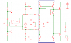
Can you show me/us how exactly this was done (a schema would be nice 🙂 )
Regards,
Frans.
what about swapping the Vbe transistor to the other polarity output device?
Or
Mount the Vbe to the Collector lead where it exits the plastic package. SMD work well here.
Or
Adopt a two Vbe multiplier, one PNP and the other NPN. Then you can monitor the Collector lead temperature of both output polarities.
Or
Mount the Vbe to the Collector lead where it exits the plastic package. SMD work well here.
Or
Adopt a two Vbe multiplier, one PNP and the other NPN. Then you can monitor the Collector lead temperature of both output polarities.
Last edited:
Hi all,
I am starting the build.
Some simple questions please.
1) So I matched the hfe of Q1 and Q2 with most of this around 650 to 700?
2)The hfe of Q3 and Q4 and most of this around 400 to 450?
3)How close should be the matching ?
4)What about Q6 and Q7? Does this need to be matched to Q1/2 and Q2/3?
the schematic is attached.
Thanks for the help.
I am new into this and only know how to follow instructions !
kp93300
Attachments
Can you show me/us how exactly this was done (a schema would be nice 🙂 )
Regards,
Frans.
Sure. My pleasure.
Attachments
Shaan, using the MOSFETS does not really need a Vbe multiplier and I biased my with just a simple diode. Two will take it into high biased class AB and operate in class A for most of the time except you dissipate a lot of necessary watts. class A.
The amp is a little quirky at start-up but stabilizes after a little while, it is best to set off-set and bias when the temperature settles. In other words set, wait adjust, and repeat a few time to get a stable setting. No matter how hard you try to match the trannies, PNP and NPN behaves slightly different and I have not bothered to match anything in my set-up, to me it is a bit of a waste of time, I listen to it mostly not measure it.
The amp is a little quirky at start-up but stabilizes after a little while, it is best to set off-set and bias when the temperature settles. In other words set, wait adjust, and repeat a few time to get a stable setting. No matter how hard you try to match the trannies, PNP and NPN behaves slightly different and I have not bothered to match anything in my set-up, to me it is a bit of a waste of time, I listen to it mostly not measure it.
Shaan, using the MOSFETS does not really need a Vbe multiplier and I biased my with just a simple diode. Two will take it into high biased class AB and operate in class A for most of the time except you dissipate a lot of necessary watts. class A.
The amp is a little quirky at start-up but stabilizes after a little while, it is best to set off-set and bias when the temperature settles. In other words set, wait adjust, and repeat a few time to get a stable setting. No matter how hard you try to match the trannies, PNP and NPN behaves slightly different and I have not bothered to match anything in my set-up, to me it is a bit of a waste of time, I listen to it mostly not measure it.
I know Nico, that I don't need the vbe multiplier. But current in the VAS stage is >25mA(in the opamp type, deliberate. The original SSA I built has 11mA of VAS current) and I don't like this much current flowing through pots. Also the pot-slider may occassionally disconnect from the conductive layer while turning- resulting into either blown FETs or if I'm lucky, fuses. This is not the case with the multiplier. So I left it where it is. 🙂 Using diodes is a good idea. But the multiplier approach apeals to me, even though the transisitor is placed on-board(as latfets has +ve tempco).
SSA is a pleasure to listen to. NO complains. I know the problems I faced is just an isolated case. I'll find a way 'round.
- Status
- Not open for further replies.
- Home
- Amplifiers
- Solid State
- Simple Symetrical Amplifier