Happy camper 🙂
Hi guys,
another successful build!
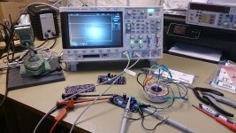
I got my three boards from OSH Park two days ago. Two boards assembled, one soldered up and tested. The Mouser BOM I uploaded is great except that the 2xN socket row is not ideal. I'll try to find something better. The 220uF caps fit just great.
Please don't forget to read the Quasimodo_jig_revA.pdf from Marks' first post. It has good points on rectifier selection.
Thanks a lot for your great work!
Børge
Hi guys,
another successful build!
I got my three boards from OSH Park two days ago. Two boards assembled, one soldered up and tested. The Mouser BOM I uploaded is great except that the 2xN socket row is not ideal. I'll try to find something better. The 220uF caps fit just great.
Please don't forget to read the Quasimodo_jig_revA.pdf from Marks' first post. It has good points on rectifier selection.
Thanks a lot for your great work!
Børge
Attachments
Børge, congratulations on your success! You made your own PCBs, created your own Bill Of Materials, purchased components yourself, assembled some Quasimodo boards, and they worked well: Bravo. Your Can-Do attitude produced a victory.
Now it's time to learn how to use that USB socket on the front panel of your Agilent scope, to save screen images to thumb-drive "disk" .
Now it's time to learn how to use that USB socket on the front panel of your Agilent scope, to save screen images to thumb-drive "disk" .
Well Mark, my dirty little secret is that I do this kind of stuff for a living 🙂 Check out the DAC link in my signature to see more of what I do.
Coming to your set table was a joy. To try make up for it I'll buy you a beer next time I'm in your neighborhood.
Børge
Coming to your set table was a joy. To try make up for it I'll buy you a beer next time I'm in your neighborhood.
Børge
My Quasimodo in action
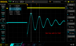
Another build, but from a newbie this time, thanks Mark for this nice tool. R=79.2ohm when I get the second picture.


Another build, but from a newbie this time, thanks Mark for this nice tool. R=79.2ohm when I get the second picture.
Very nicely done, cwtim01! Congratulations on your success. That's quite a nice looking, optimally-snubbed waveform.Another build, but from a newbie this time, thanks Mark for this nice tool. R=79.2ohm when I get the second picture.
But I'm not sure it's such a good idea to socket the MCP1407 gate driver IC. With Iout = 6 amperes, its dI/dt has got to be incredibly large, so you want the minimum possible inductance in its I/O pins & supply pins. Sockets increase, rather than decrease, inductance.
Last edited:
I am very new to the DIY website. I have enjoyed audio for many years and make my living doing it. I am excited to see the range of skills and knowledge when it comes to building the various components in a home sound system. Growing up I enjoyed building many Heathkits, some of which still work today in my home!
Mark's Quasimodo project looks like the perfect way to get back into the building of a sound system. I have ordered one of the Salas shunt regulator boards with some of the parts from "Teabag" as a step towards building a BA-3 preamp.
Having the ability to improve on the supply and sound would be great.
So, are there any boards for this project still out there, or would a group buy be a good thing. I am willing to place the order, if Mark's offer still stands for sharing the files necessary to create the PCBs.
Thoughts and comments are welcomed.
Tnx
David Rogers
Nashvegas
David, all files are attached to post #1 of this thread. In post #1 you can read the (long!) list of diyAudio members who have already downloaded those files, used the files to order PCBs from either Seeed Studio or OSH Park, and then built themselves a working Quasimodo. It can be done. Others have tried and succeeded. Good luck!
But I'm not sure it's such a good idea to socket the MCP1407 gate driver IC. With Iout = 6 amperes, its dI/dt has got to be incredibly large, so you want the minimum possible inductance in its I/O pins & supply pins. Sockets increase, rather than decrease, inductance.
Thanks for the tips about the socket, they're there only because I'm still not very comfortable with my soldering skills yet. Given your comment I'll try taking them away.
BTW, I have a few spare v4 boards printed by Seeed with ENIQ (gold plated pads) finish, interested ones can send me a PM, happy to part with them at USD9 per board + shipping.
Last edited:
It surprises me that many people who you would expect to know better do not understand that it is the resistor that does the snubbing and not the capacitor ---- It depends, I saw few so-called lossless snubbers that worked very well. Capacitor, inductor and diod. What is does it stores energy when you close your transistor than gives it back. Due to process time it reduces spike. That is it, no magic.
Final point is that the snubber components need to be located as close to the transformer as possible for the best results ---- That is obvious. Close you place, less parasite element introductory.
Final point is that the snubber components need to be located as close to the transformer as possible for the best results ---- That is obvious. Close you place, less parasite element introductory.
Attachments
Last edited:
Thanks, CWTim01. Mark inspired me to place an order for boards, so I ordered three from OSH Park, which means I will have two left over. Just finished placing an order with Digikey for all of the bits and pieces needed to populate the board. I went ahead and ordered three sets of everything. If someone out there wants a complete kit of board and parts, I will have two sets. I will just be happy to recoup the cost.
Thanks
David
Nashvegas
Thanks
David
Nashvegas
Since the board appears to be working fine, I'd leave it alone, and promise myself to omit the socket from the other two boards. This board works fine, the other two will work even better. I don't know about you but my soldering skills are such that desoldering a DIP-8 socket then resoldering a DIP-8 IC package in its place, has only a 70% chance of success. Whereas doing nothing at all has a 100% chance of success. You could always give away or sell the socketed board.Thanks for the tips about the socket, they're there only because I'm still not very comfortable with my soldering skills yet. Given your comment I'll try taking them away.
You could put your scope probe on the DRAIN node (driven end of Cx) and look for non-flatness right after the falling edge; that would indicate excess inductance in the pulldown current loop. This kind of non-flatness is visible in the "Blue Ring" scope photo on page 8: see the bottom portion of trace B (LINK) Do this measurement with zeta = 0 (Rs removed from its socket) and again with zeta = 1 (Rs = optimum).
Since the board appears to be working fine, I'd leave it alone, and promise myself to omit the socket from the other two boards.
OK, so I made a second one 😀
If measurement error is accounted for, the optimum R obtained from both units is practically the same (79.2 vs 78.8 ohm) for the same toroid, and I suppose the socketed one is still good then 🙂

Hi guys,
perhaps a bit OT, but probably relevant. In Mark's paper on the Quasimodo (post #1) he mentions his belt and suspenders approach to snubbing and rectifying.
Today I came across these cuties:
Cree C3D1P7060Q
The Cree SiC diodes are nicely priced, most of them come in 2-pin TO220 packages which are trivial to solder. I'll try to gain access to the tools required to solder the 3x3mm QFNs.
What do you think about building SiC based rectifiers for audio projects?
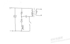
Another thing: Any opinions about using an inductor in series with the large smoothing capacitor on the DC side of the rectifier bridge? The purpose is to lower the peak current in the transformer. That would be the bottom-right configuration at:
http://www.hammondmfg.com/pdf/5c007.pdf
I'll receive samples of the 1400uH inductor in:
http://www.coilcraft.com/pdfs/do5040h.pdf
I'll let you know when I get it patched up. Actually, starting with correct snubbing, there is a lot we can do to improve on the standard mains-trafo-rectifier-LDO style of PSU!
Børge
perhaps a bit OT, but probably relevant. In Mark's paper on the Quasimodo (post #1) he mentions his belt and suspenders approach to snubbing and rectifying.
Today I came across these cuties:
Cree C3D1P7060Q
The Cree SiC diodes are nicely priced, most of them come in 2-pin TO220 packages which are trivial to solder. I'll try to gain access to the tools required to solder the 3x3mm QFNs.
What do you think about building SiC based rectifiers for audio projects?
Another thing: Any opinions about using an inductor in series with the large smoothing capacitor on the DC side of the rectifier bridge? The purpose is to lower the peak current in the transformer. That would be the bottom-right configuration at:
http://www.hammondmfg.com/pdf/5c007.pdf
I'll receive samples of the 1400uH inductor in:
http://www.coilcraft.com/pdfs/do5040h.pdf
I'll let you know when I get it patched up. Actually, starting with correct snubbing, there is a lot we can do to improve on the standard mains-trafo-rectifier-LDO style of PSU!
Børge
I haven't seen any manufacturer measurements or datasheet-guaranteed specifications of the "softness" (tb/ta) of SiC diodes. Nor have I made any measurements upon SiC diodes myself.
My personal decision has been to buy from manufacturers who (a) measure, and (b) specify, and (c) guarantee this soft-recovery parameter. Fairchild is one (example); notice the sortable column called tb/ta. Recently I purchased 100 pcs of their FFPF30UP20S (30A, 200V, soft recovery) for use in DIY solid state equipment. The price was not unacceptable. I used octopart to find the best deal among reputable, non-counterfeit, manufacturer-approved distributors. This diode's 200V rating would be inadequate for valve gear, of course.
My personal decision has been to buy from manufacturers who (a) measure, and (b) specify, and (c) guarantee this soft-recovery parameter. Fairchild is one (example); notice the sortable column called tb/ta. Recently I purchased 100 pcs of their FFPF30UP20S (30A, 200V, soft recovery) for use in DIY solid state equipment. The price was not unacceptable. I used octopart to find the best deal among reputable, non-counterfeit, manufacturer-approved distributors. This diode's 200V rating would be inadequate for valve gear, of course.
That's interesting. I've been looking at their FFPF60SA60DSTU to save space but I haven't yet looked at the finer details of how to select this kind of diode.
Børge
Børge
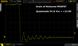
Here are a couple of edge rate measurements, made on a V4 thru-hole board with a NTD4906 MOSFET, 13.9 volt supply, MCP1407 gate driver IC, and injection capacitor Cx = 0.01 uF. Both photos have 2.0 volts per vertical division, and 10.0 nanoseconds per horizontal division.
Eyeball estimation says the gate risetime is ~ 30 nsec, and the drain falltime is ~ 3 nsec.
Eyeball estimation says the gate risetime is ~ 30 nsec, and the drain falltime is ~ 3 nsec.
Attachments

Hello everybody,
I've been reading diyAudio for some time, and found quite a lot of useful information. Having myself acquired a bit of knowledge on the subject of transformer snubbing, I would like to share it on the forum.
Having recently built a RIAA preamp, I started buliding a power supply for it based on the Jung/Didden superreg (thanks for the nice PCB, Jan). Having read the article by M. Jones on rectifier snubbing in Linear Audio Vol. 5 i decided to investigate the subject further, and built the Quasimodo jig in the process (NE555, TC4427 MOSFET driver & IRFD020 as switch).
However, the transformer I picked for the project (German-made,
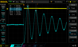
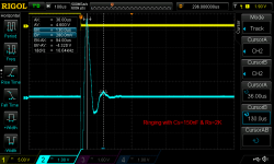
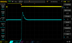
Spitznagel brand, vacuum potted, split-primary, split secondary 2x18V, 389 mA) proved a difficult one to tame. Using the Quasimodo jig, I measured a natural frequency of 11.36kHz with Cx=10nF & Rs=inf.(leftmost figure), and 3kHz with Cx=10nF & Cs=150nF & Rs=0 (2nd fig. from the left), but it was impossible to see it ringing with Cs=150nF and Rs=1K. Damped ringing was observed with Rs=2K (3rd fig.). There was no clear-cut position of the point with optimal secondary damping; the result shown for Rs=750R in 4th fig. from the left was estimated visually. Reducing further the value of Rs (overdamping, as Mark termed it in post #143) moved the system towards the natural frewuency of 3kHz.
My interpretation of this behaviour is that we dealing here with a system with two natural frequencies; and Rs is the element that positions the operating point with regard to ringing between the two natural modes defined by Cx=10nF and Cx+Cs=160nF. In the optimal point, both modes are damped; moving leftwards or rightwards from this point overdamps the one mode and underdamps the other one. This is so because the CRC snubber works on a detuned transformer secondary, the detuning being effected by the capacitor Cx.
The adjustment range of Rs where neither of the modes is visible is between 500 and 800 Ohm in this particular case. So setting Rs=650R provides safety margins on both sides of this value.
I've been reading diyAudio for some time, and found quite a lot of useful information. Having myself acquired a bit of knowledge on the subject of transformer snubbing, I would like to share it on the forum.
Having recently built a RIAA preamp, I started buliding a power supply for it based on the Jung/Didden superreg (thanks for the nice PCB, Jan). Having read the article by M. Jones on rectifier snubbing in Linear Audio Vol. 5 i decided to investigate the subject further, and built the Quasimodo jig in the process (NE555, TC4427 MOSFET driver & IRFD020 as switch).
However, the transformer I picked for the project (German-made,
Spitznagel brand, vacuum potted, split-primary, split secondary 2x18V, 389 mA) proved a difficult one to tame. Using the Quasimodo jig, I measured a natural frequency of 11.36kHz with Cx=10nF & Rs=inf.(leftmost figure), and 3kHz with Cx=10nF & Cs=150nF & Rs=0 (2nd fig. from the left), but it was impossible to see it ringing with Cs=150nF and Rs=1K. Damped ringing was observed with Rs=2K (3rd fig.). There was no clear-cut position of the point with optimal secondary damping; the result shown for Rs=750R in 4th fig. from the left was estimated visually. Reducing further the value of Rs (overdamping, as Mark termed it in post #143) moved the system towards the natural frewuency of 3kHz.
My interpretation of this behaviour is that we dealing here with a system with two natural frequencies; and Rs is the element that positions the operating point with regard to ringing between the two natural modes defined by Cx=10nF and Cx+Cs=160nF. In the optimal point, both modes are damped; moving leftwards or rightwards from this point overdamps the one mode and underdamps the other one. This is so because the CRC snubber works on a detuned transformer secondary, the detuning being effected by the capacitor Cx.
The adjustment range of Rs where neither of the modes is visible is between 500 and 800 Ohm in this particular case. So setting Rs=650R provides safety margins on both sides of this value.
Attachments
DNi, your oscillation frequencies are astoundingly low, which implies an astoundingly high secondary leakage inductance.
If Lsecondary really and truly IS 19 milliHenrys, then with Cx=10 nanoFarads and Cs=150 nanoFarads, critical damping (zeta=1.00) occurs at Rs = 690 ohms. {Quasimodo design note equation (A.11)}
- A parallel LC circuit with C= 10 nanoFarads and L= 20 milliHenrys, resonates at 11.4 kHz. {equation (A.10)}
- A parallel LC circuit with C= 160 nanoFarads and L= 17 milliHenrys, resonates at 3 kHz. {(A.10)}
If Lsecondary really and truly IS 19 milliHenrys, then with Cx=10 nanoFarads and Cs=150 nanoFarads, critical damping (zeta=1.00) occurs at Rs = 690 ohms. {Quasimodo design note equation (A.11)}
Attachments
Last edited:
Thank you for your comment, Mark.
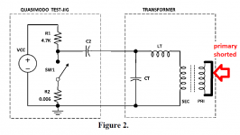
Based on the data acquired, the leakage inductance is 18.8mH. The primary windings are connected in series (230V operation) and then shorted. The other secondary is also shorted.
I see similar leakage inductance in Fig. 17 of your paper (17.1 mH), but I did not check the numbers.
I wondered myself as to the numbers, but so far I could not find an error.
- Home
- Amplifiers
- Power Supplies
- Simple, no-math transformer snubber using Quasimodo test-jig