Hello,
Thank you branadic.
Yes, in the final design i will use two ADCs and DACs.
They can be used in many different way. With interleaving we can get twice sampling rate, or with simultaneous sampling and averaging we can increase the SNR.
Two channels are very important also if we want to compute two signals between us (bode plot).
You are right, there is a lot of end application possible.
Anyway, i will only write the code that fit for my own need, and any interested user will need to write it's own CPLD firmware for it's intended use.
I wait some digital isolators right now to connect the SDRwidget on the system.
But as i work on others things, there is now major update for now.
Regards.
Frex
Hi Frex! Great work and great project! Very very interesting. What is the fate and current state of the project? Tell me please, did you consider new chips and boards: 1.LTC2508-32 http://cds.linear.com/docs/en/datasheet/250832fc.pdf http://cds.linear.com/docs/en/demo-board-manual/dc2222afa.pdf 2. ADS127L01 http://www.ti.com/lit/ds/symlink/ads127l01.pdf http://www.ti.com/lit/ug/sbau261b/sbau261b.pdf 3. LTC2500-32 http://www.linear.com/docs/en/datasheet/250032fa.pdf http://cds.linear.com/docs/en/demo-board-manual/DC2390AF.PDF as candidates for building a measuring ADC? Characteristics of them look very attractive IMHO. Regards Igor
Hello,
As you Igor, i looked much on high performance ADC from all manufacturers.
These ADC are also very good, but not seem to reach the LTC2380-24 at this level of sampling rate.
I don't have made much job on the project these last weeks.
Anyway my AT2380 attenuator project is now done (i will use it for the ADC),
so i will continue on the ADC project now.
I've made an isolator board to send the I2S datas from the FPGA board to the
USB widget board.
That will offer direct isolated USB connexion to the ADC with open source firmware.
I must also see about the analog input stage, i think to ask to DIYers what target inputs specs would be the better.
I think to start a whole schematic design for prototype at start of next year.
Regards.
Frex
Hi Frex! Thanks! Yes, the frequency range of these ADC chips is less than 2380-24, but it allows to work with sampling frequencies of 384 and 768 kHz. This is sufficient for measuring audio devices in general. Best Igor
In my experience these input levels seem to work well: 300 mV, 3V, 30V, 300V.
However it's never so simple. With your attenuator and a really good analog circuit you should be able to ideally AGC the input to the optimum of the ADC. This is how most of the good analog boxes work. The huge dynamic range makes moving the level stuff to the digital side look promising but in virtually any system I have checked (analog or digital) the optimum trade out between distortion and noise seems to be 10-15 dB below full scale with a 5 db min-max before the performance degrades. I don't know enough about that SAR but I would be surprised if it was a lot different.
However it's never so simple. With your attenuator and a really good analog circuit you should be able to ideally AGC the input to the optimum of the ADC. This is how most of the good analog boxes work. The huge dynamic range makes moving the level stuff to the digital side look promising but in virtually any system I have checked (analog or digital) the optimum trade out between distortion and noise seems to be 10-15 dB below full scale with a 5 db min-max before the performance degrades. I don't know enough about that SAR but I would be surprised if it was a lot different.
Start of project : OSVA "Open Source Versatile Analyzer"
Hello all,
After some time to think (and some holidays too), i had progress on define what would be a real analyzer
design from my previous work with the LTC2380-24 ADC.
The name of this analyzer project is OSVA as "Open Source Versatile Analyzer"
I define first a specs for this design ;
-- DIY friendly build (as possible).
-- Open source hardware and software, to allow users to contribute to the platform development.
-- High performance and versatile design.
-- Modular for fitting to users needs
With this, the analyzer would be build using up to 5 different PCB ;
1) AA2380 ADC PCB -(2 channels ADC board) with :
Two channels high performance analog front-end (AFE).
Two LTC2380-24 24 bits 1.6MSPS ADC
ADC voltage references
Low noise Voltage regulators (power supply)
ADC low jitter clock
A small CPLD for logic interface
2) AA10MXX LOGIC PCB - (digital board) with :
Intel 10MXX CPLD
Dual Clock oscillators
High-Speed I/O connectors
Voltage regulators
Isolated I/O interfaces for SDR-widget and USB-streamer
LCD display interface connectors (HDD44780 compatible)
Rotary encoder input
Connector for future DAC PCB.
(and more TBD...)
3) AAPSU01 - Low noise power Supply PCB
Generate voltage for AA2380 and AA10M08 from
a single 12V source.
(only Small wall adapter required)
4) SDR Widget - (CPU board only)
Already existing design from George Bourdeau (Open source).
This I/O card allow 24 bits/192kHz (AD+DA )data transfer operation
via USB link (Class 2 audio device). Link to analyzer is isolated.
5) USB-Streamer - Third party I2S to USB (Proprietary design)
Connecting USB streamer to AA10M08 allow 24/192 kHz on 4 channels
used to reconstruct 24 bits 768KHz sampling rate.
(require compatible software)
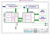
The preliminary functional synoptic of the OSVA can be show on file below :
-- OnE Audio Projects // OSVA preliminary functional synoptic --
This hardware configuration allow several user configurations.
Indeed, there is multiple building options :
The AA2380 PCB alone provide some direct digital interfaces :
isolated stereo S/PDIF OUTPUT (stereo)
Sampling rate selection : 48/96/192 KHz operation
Sinc digital Averaging filter ratio selection switch : x32 to x1
Isolated I2S output (up to 1.536 MSPS)
Buffered clock output
Direct connexion to SDR-Widget or USB-streamer(*) for USB output.
So, some user can only work with this board.
The AA10M08 PCB allow to extend signal processing and
add some GUI feature with LCD screen and a rotary encoder.
It provide also two fast isolated extension port to send data
to "SDR-Widget" and "USB-streamer" USB adapter board.
So the interface allow stereo 24 bits 768kHz or mono
24 bits 1536 kHz operation by using the four 24/192 channels
of the USB-streamer board and concatenating them in a single stream.
(Require compatible software like HpWorks).
The CPLD include FIR brick-wall filtering to avoid spectral aliasing.
Because all the CPLD code will be open sourced and available on Github,
writing your own filter is possible.
The LCD screen display in real time main input frequency and
input signal peak amplitude in dBFS.
It display also filter type selection (FIR,SinC, others), averaging ratio and more...
All settings are controlled with a rotary encoder and it's push button.
The SDR-widget and USB-streamer(*) are optional solutions to provide direct USB
connexion for the analyzer.
For both ,the USB ground is fully isolated from the analyzer ground to avoid loop issue and noise.
The AAPSU01 is a board that provide all required voltage to AA2380
and AA10M08 for proper operation from a single wall-mount 12V adapater ( low noise type).
The SDR-Widget and USB-streamer are itself self-powered from USB power.
* : USB-Streamer require a little hardware modification to be used with analyzer
master clock.
Of course, if others hardware interfaces are available to transfer data, it would
be great that they can be used in the analyzer (even if not open sourced, but available for DIYers).
I think about the XMOS design of JenSH in it's analyzer, and also on the current work of Mkc.
This is a first attempt to define the analyzer, and i hope that satisfy much DIYers needs.
It also a first step before to start the first PCB design of the analyzer, the AA2380.
Any opinion and advice are welcome. Thank you.
Regards.
Frex
Hello all,
After some time to think (and some holidays too), i had progress on define what would be a real analyzer
design from my previous work with the LTC2380-24 ADC.
The name of this analyzer project is OSVA as "Open Source Versatile Analyzer"
I define first a specs for this design ;
-- DIY friendly build (as possible).
-- Open source hardware and software, to allow users to contribute to the platform development.
-- High performance and versatile design.
-- Modular for fitting to users needs
With this, the analyzer would be build using up to 5 different PCB ;
1) AA2380 ADC PCB -(2 channels ADC board) with :
Two channels high performance analog front-end (AFE).
Two LTC2380-24 24 bits 1.6MSPS ADC
ADC voltage references
Low noise Voltage regulators (power supply)
ADC low jitter clock
A small CPLD for logic interface
2) AA10MXX LOGIC PCB - (digital board) with :
Intel 10MXX CPLD
Dual Clock oscillators
High-Speed I/O connectors
Voltage regulators
Isolated I/O interfaces for SDR-widget and USB-streamer
LCD display interface connectors (HDD44780 compatible)
Rotary encoder input
Connector for future DAC PCB.
(and more TBD...)
3) AAPSU01 - Low noise power Supply PCB
Generate voltage for AA2380 and AA10M08 from
a single 12V source.
(only Small wall adapter required)
4) SDR Widget - (CPU board only)
Already existing design from George Bourdeau (Open source).
This I/O card allow 24 bits/192kHz (AD+DA )data transfer operation
via USB link (Class 2 audio device). Link to analyzer is isolated.
5) USB-Streamer - Third party I2S to USB (Proprietary design)
Connecting USB streamer to AA10M08 allow 24/192 kHz on 4 channels
used to reconstruct 24 bits 768KHz sampling rate.
(require compatible software)
The preliminary functional synoptic of the OSVA can be show on file below :
-- OnE Audio Projects // OSVA preliminary functional synoptic --
This hardware configuration allow several user configurations.
Indeed, there is multiple building options :
The AA2380 PCB alone provide some direct digital interfaces :
isolated stereo S/PDIF OUTPUT (stereo)
Sampling rate selection : 48/96/192 KHz operation
Sinc digital Averaging filter ratio selection switch : x32 to x1
Isolated I2S output (up to 1.536 MSPS)
Buffered clock output
Direct connexion to SDR-Widget or USB-streamer(*) for USB output.
So, some user can only work with this board.
The AA10M08 PCB allow to extend signal processing and
add some GUI feature with LCD screen and a rotary encoder.
It provide also two fast isolated extension port to send data
to "SDR-Widget" and "USB-streamer" USB adapter board.
So the interface allow stereo 24 bits 768kHz or mono
24 bits 1536 kHz operation by using the four 24/192 channels
of the USB-streamer board and concatenating them in a single stream.
(Require compatible software like HpWorks).
The CPLD include FIR brick-wall filtering to avoid spectral aliasing.
Because all the CPLD code will be open sourced and available on Github,
writing your own filter is possible.
The LCD screen display in real time main input frequency and
input signal peak amplitude in dBFS.
It display also filter type selection (FIR,SinC, others), averaging ratio and more...
All settings are controlled with a rotary encoder and it's push button.
The SDR-widget and USB-streamer(*) are optional solutions to provide direct USB
connexion for the analyzer.
For both ,the USB ground is fully isolated from the analyzer ground to avoid loop issue and noise.
The AAPSU01 is a board that provide all required voltage to AA2380
and AA10M08 for proper operation from a single wall-mount 12V adapater ( low noise type).
The SDR-Widget and USB-streamer are itself self-powered from USB power.
* : USB-Streamer require a little hardware modification to be used with analyzer
master clock.
Of course, if others hardware interfaces are available to transfer data, it would
be great that they can be used in the analyzer (even if not open sourced, but available for DIYers).
I think about the XMOS design of JenSH in it's analyzer, and also on the current work of Mkc.
This is a first attempt to define the analyzer, and i hope that satisfy much DIYers needs.
It also a first step before to start the first PCB design of the analyzer, the AA2380.
Any opinion and advice are welcome. Thank you.
Regards.
Frex
Attachments
Could you also consider to support the the DIYINHK USB-I2S interfaces as eg this one.
These have four 384kHz channels and mention two 768kHz with customized firmware. That would allow higher rates for a wider range of software.
Moreover the connector to program the xmos is accessible, perhaps someone can bring it to two 1536kHz channels by using the resources of the unneeded USB to I2S part.
I would love see a high quality programmable clock (e.g. a Si545).
One reason would be that the sample frequency could be fine tuned to match a reference coming from the DUT.
A second reason would be to get rid of the standard frequencies, then you could e.g. sample with a multiple of the test signal and use a rectangular window for analyses. This however would probably imply the need of an own USB interface being able to handle these frequencies.
Thumbs up!-- Open source hardware and software, to allow users to contribute to the platform development.
1) AA2380 ADC PCB -(2 channels ADC board) with :
Two channels high performance analog front-end (AFE).
Two LTC2380-24 24 bits 1.6MSPS ADC
What kind of analog frontend do you have in mind?
One that is designed for single ended audio line in? Or differential audio line in? Or single ended/differential selectable?
Or more geared towards test & measurement? With selectable gain, AC and DC coupling, single and differential, all modes switchable with software, jumpers or the like?
A 24 bits 1.6MSPS ADC would be a nice platform for measuring ripple and noise, higher order harmonics and so on.
If you don't need the usb audio input interface for the programs you intend to use, you could also consider using a Raspberry Pi with it's SPI interface or a Beaglebone Black with it's PRU units to read the data out of the ADC board and forward them to a PC over LAN. This would get rid of the digital and interface boards.
Hello,
Zfe,
Ok, DIYINK USB-I2S module would be used too.
Note that it's same thing as USB-Streamer, it require I2S streams.
Note that for both (and even the SDR widget) hardware need to be modified
because the main clock source come from ADC board itself.
This allow to better possible performance.
Of course, it would be probably possible to use clock from USB board but
really not sure that the better way.
Anyway, i want to do the best to allow various user interconnections.
(A main clock frequency is 98.304 MHz is required because reading 24 bits data
with SPI link of ADC at 1.536 MSPS need this ).
Note that the ADC clock will could come from external reference clock source,
but at right frequency.
electronic eel,
Thank you.
The real contain of the front end is in study for now,
but i will publish very soon the full detailed synoptic of the first AA2380 PCB (drawing in progress).
I can say that in my mind, the ADC board would include a very clean fully differential front-end
with very low noise and THD performance that don't compromise ADC specs.
It would work indifferently with single-ended or differential signals.
I have in mind too, that many users use already some external tools to make
amplitude level the best for THD measurements (Auto-ranger or my AT2380 attenuator and probably others..).
I think that another board could be designed (in second step) to be interfaced
with ADC board to provide an extended analog front end functionality as :
Auto range level with 300mV,3V,30V and 300V.
High or low input impedance mode
AC/DC coupling mode
Over-voltage protection in all range
And maybe more...
(others idea are welcome)
Separate the function allow also to make the construction cost much lower
if you don't require such front-end.
Actually, i try to separate the different functions in the analyzer to let the DIYer choose what he really need.
Using a Raspberry pi is a great idea !
The ADC board can send multiple I2S stream (at any sample rate up to 1536k)
so interfacing with the raspberry pi shouldn't be an issue.
So, if you want to help you're welcome.
Regards.
Frex
It seems that my hope to build a field recording ADC with this might not be such a good idea?
//
//
It seems that my hope to build a field recording ADC with this might not be such a good idea?
Why not ?
Frex
Progress and ideas look great Frex! 
I don't think the Raspberry Pi has an i2s input interface; only an output. What might be handy for interfacing to single board computers like Raspberry Pi (I've got a parallella here that I'm thinking of connecting to for example) would be an SPI output. I believe RPi supports up to 125MHz SPI connection.
This I guess would be possible by re-purposing some of the IO pins from the i2s port if IO on the CPLD becomes a limitation?
Another thought - wouldn't it be better to move the isolators to the ADC board to remove the potential for noise from say the LCD and other components potentially getting in to the analyser? This would mean also isolating any control comms to the ADC also. I understand that this shouldn't be a big issue with good layout, but since this is a sensitive environment ...
Cheers,
Chris
Using a Raspberry pi is a great idea !
The ADC board can send multiple I2S stream (at any sample rate up to 1536k)
so interfacing with the raspberry pi shouldn't be an issue.
So, if you want to help you're welcome.
I don't think the Raspberry Pi has an i2s input interface; only an output. What might be handy for interfacing to single board computers like Raspberry Pi (I've got a parallella here that I'm thinking of connecting to for example) would be an SPI output. I believe RPi supports up to 125MHz SPI connection.
This I guess would be possible by re-purposing some of the IO pins from the i2s port if IO on the CPLD becomes a limitation?
Another thought - wouldn't it be better to move the isolators to the ADC board to remove the potential for noise from say the LCD and other components potentially getting in to the analyser? This would mean also isolating any control comms to the ADC also. I understand that this shouldn't be a big issue with good layout, but since this is a sensitive environment ...
Cheers,
Chris
Hello,
Using SPI instead of I2S for Raspberry Pi interface shouldn't be a problem.
You are right, by using a proper CPLD firmware we can use I/O for needed purpose.
About the isolating, it's not yet decided. I must think more about this.
But IMHO, the specific use of the R pi with the AD board can be done by adding small
specific isolating interface. That don't force others user to paid for the isolator on the AD PCB if not required..
Frex
I like using a standalone processor (Rasberry Pi or BB Black) to run it as a test instrument. You can also then load software to do specific preprocessing. Isolation then is an issue of the power supplies isolation if using wifi for comm and control. If the processor runs Linux lots of useful stuff is available. Usually I/O interfaces on these are quite programmable in the sense that I2S is software created. You definitely don't want the processor to be the clock source. Transformer isolated clocks can work very well if you need that level of isolation.
However I feel strongly that an associated source should not share a ground with the ADC side. That always leads to unintended ground loops.
However I feel strongly that an associated source should not share a ground with the ADC side. That always leads to unintended ground loops.
Hello,
Using SPI instead of I2S for Raspberry Pi interface shouldn't be a problem.
You are right, by using a proper CPLD firmware we can use I/O for needed purpose.
About the isolating, it's not yet decided. I must think more about this.
But IMHO, the specific use of the R pi with the AD board can be done by adding small
specific isolating interface. That don't force others user to paid for the isolator on the AD PCB if not required..
Frex
You could also consider something like FT600Q or a slower version for data output via USB at higher than audio rates. I think the FTDI APIs are widely used enough you may find off-the-shelf software or plugins that can work.
Another possibility is the SoC chips from Altera or Xilinx. Dual core ARM Cortex-A9 and FPGA in one package.
Terasic and Digilent have some nice development boards for 100$.
Terasic and Digilent have some nice development boards for 100$.
In case you consider SoC, or FPGA, you shall take into consideration to develop the board in an FMC form or similar. (FPGA mezzanine card). Many FPGA developer boards are available (like Opal Kelly), you just need to create the precious analog frontend; the post-processing, lan/USB connectivity, display can be done in the FPGA devel board. (where lots of IP is available, like high speed USB3 connection, etc. Check the FPGA devel board vendor website to see, what is available)
Hi all,
I think that if the ADC board (AA2380) include a CPLD, interfacing it to send data
to almost any hardware like Raspberry-pi, SoC board , and more will not be an issue.
If isolation is required (and i know that it's often), then an isolation PCB can be added.
I understand that adding another PCB is not always satisfying, but it's the price for
some modularity of the system.
Demian,
As you, I would be very happy if the analyser could work fully in stand-alone mode
using a R-pi or others CPU boards, but there is a big software job (and not in my skill).
So, we will need to find some skilled team for that 🙂 .
(It's a foot call)
Chris,
You are right, the FT600 seem good solution to get high speed data rate from USB.
I think we can also seen FT600 USB link as a dedicated board that can be interconnected with the AA10M08 logic board.
Note that there is also some software to write for collecting data on computer side,
and the FTDI chip driver is not recognized as audio device.
So it is not so easy to use our usual audio softwares.
meszarosa,
About the PCB interconnect, i know that FMC connector is fine for their density and bandwidth,
but the very fine pitch and a bottom soldering make them problematic for a DIY project.
No obvious to decide for now... I keep it in mind.
Frex
Chris,
You are right, the FT600 seem good solution to get high speed data rate from USB.
I think we can also seen FT600 USB link as a dedicated board that can be interconnected with the AA10M08 logic board.
Note that there is also some software to write for collecting data on computer side,
and the FTDI chip driver is not recognized as audio device.
So it is not so easy to use our usual audio softwares.
Frex
Should not USB2 be fast enough?
If I made no error, we need about 13 MBps here and USB2 should reach about 40MBps available for the user.
- Home
- Design & Build
- Equipment & Tools
- SAR ADC for high performance audio ADC project [LTC2380-24]