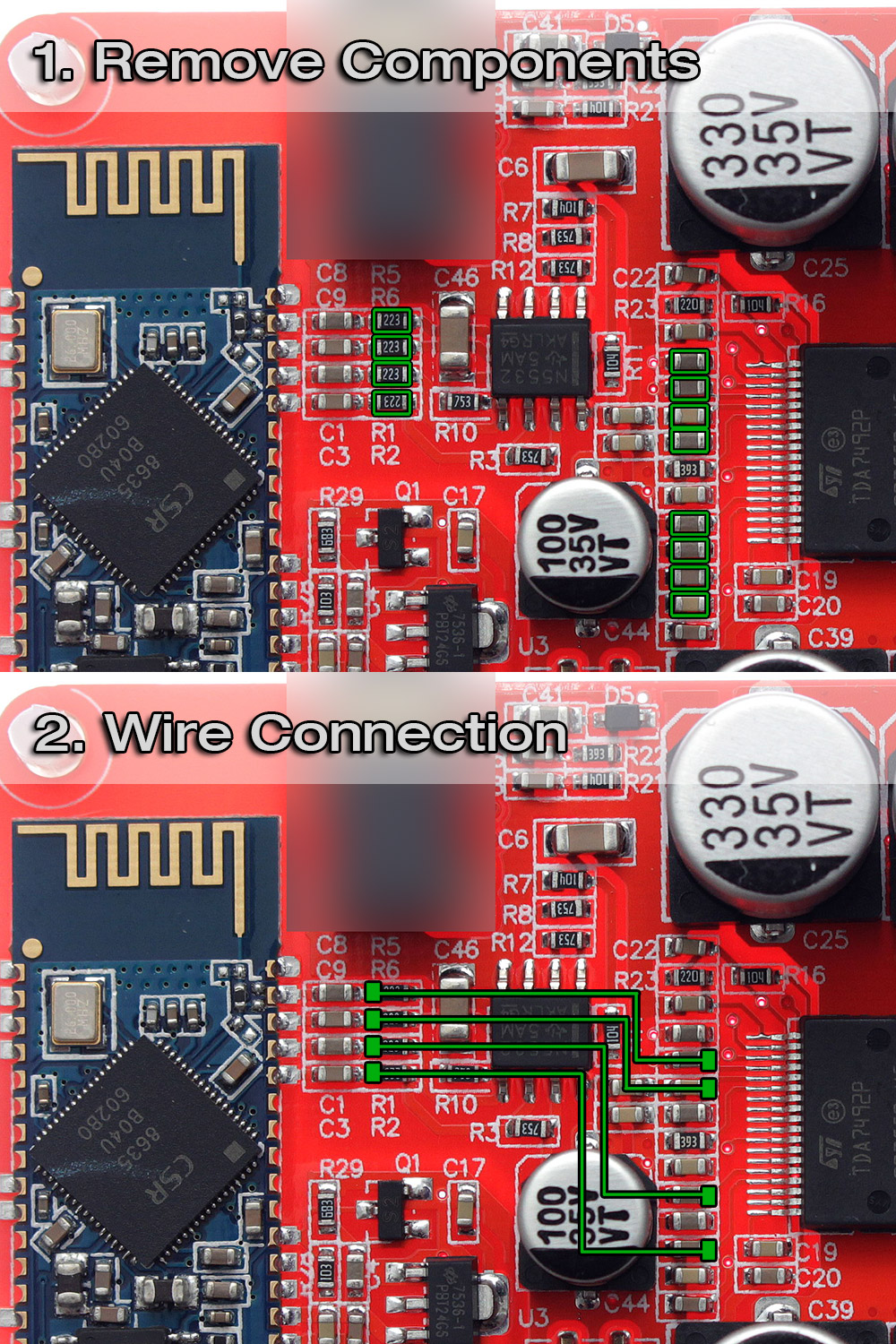
Greetings everyone. I looked at the datasheets for the components and came up with this mod for the board I have. Can someone check my work? I'm not an electronics engineer 😀
I do remember for some reason the polarity was inverted on one channel when I tested this amp. Anyone have an idea where the polarity swap is on the board? My eyes are not sharp enough to see where.

I do remember for some reason the polarity was inverted on one channel when I tested this amp. Anyone have an idea where the polarity swap is on the board? My eyes are not sharp enough to see where.
The polarity swap is at the BT module and can be seen from the bottom side traces. Your fix is quite good but lacks fixing the GND-connection at TPA inputs.

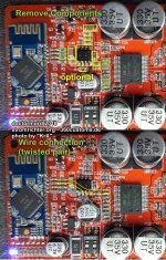
I own the red PCB, and i noticed a difference in the mod as seen here above, and a mod in another post.
the difference is between the wired connections
and
which mod is the right one?
the difference is between the wired connections
Try this:
Untested, but should do.
and
And the other one:
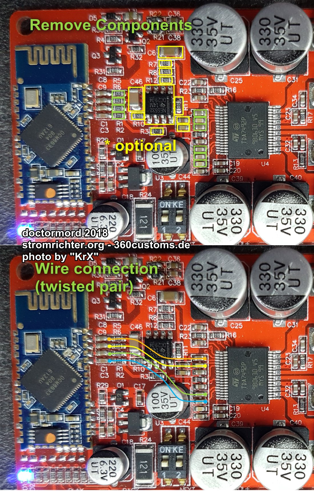
which mod is the right one?
which mod is the right one?
When you look closely, those are two different layouts, but the fix is basically the same. Check the input pins in the bottom left corner of the IC and follow the traces, you can see the difference then.
Yes i see it now, sorry
In the upper picture it was difficult to see the connection to the chip.
In the upper picture it was difficult to see the connection to the chip.
so i tested it out and the HISS sound is nearly gone (when i watch that youtube video i posted earlier). now i need to get next to the speaker to hear it.
the loudness is not as loud as before but i think thats ok
so thanks for your help.
now i just want to know why the opamp is there from the beginning if it creates that problem?
the loudness is not as loud as before but i think thats ok
so thanks for your help.
now i just want to know why the opamp is there from the beginning if it creates that problem?
The opamp is there just because they also offer pcb design implementations with aux/line-in which is single ended. To simplify the implementation, the first convert the BT module signal to single ended and then use either some resistive signal mixing or a switched 3.5mm jack, where BT signal gets switched away when a plug in inserted. There are also boards which feature some "tone control" in between the BT source and the amps input.
To keep complexity low, they leave the opamps in even when not needed. (Keeping BOM costs low due to volume ordering)
This is supposed to work if an isolated supply for at least the BT module is used. Otherwise they could have used the internal CSR ADCs to implement the line-in/aux feature by changing some programming.
(The rest is the usual "copy-cats" story and/or "let the customers do our job [research&developement]")
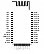
Slightly off-topic, but going through this thread (or searching diyAudio forums) I couldn't find the answer. I have one of the blue Sanwu 3116 boards with the 8635 bluetooth module. Are the SPI pins for the 8635 brought to the rightmost 4 pads of the seven pads in a row below the 8635 daughter card? If so, what is the pin assignment for these pads?

Thanks!
Thanks!
Tiny Sine has documentation on a module that looks very very similar. Here's the link: Bluetooth 4.2 APTX Audio Module
I would attach the documentation but the website does not load at my workplace (DNS issue).
I would attach the documentation but the website does not load at my workplace (DNS issue).
And the other one:
Thanks!
I finally gathered sufficient courage to fix one of these boards (my SMD-scale soldering skills are not the best). After the fix, the board does look a bit ugly, but it sounds excellent. The gain switches on the board now actually work - they didn't change the output level too much before as the opamp was probably overdriving the input to TDA7492. When I set the gain to minimum (both switches off), the status dings are not annoyingly loud, and there's no noise/hiss/static when the input is quiet. The audio quality seems to be better, too, though that could be subjective.
I can confirm the bottom pads are routed to the SPI on the CSR. I soldered leads to these pads on my "test" board. I have the pins written down, I will update when I get back to the workshop. Otherwise you can tone them out fairly easy.
I would totally encourage people to get the programming working. For the price they are amazingly capable. I am able to apply eq/filters/compression in real time while listening to music. Really fun to mess around with.
I would totally encourage people to get the programming working. For the price they are amazingly capable. I am able to apply eq/filters/compression in real time while listening to music. Really fun to mess around with.
Here are the pin outs from left to right:
1 - SPI_PCM
2 - Ground
3 - VBAT
4 - MOSI
5 - CLK
6 - CSB
7 - MISO
1 - SPI_PCM
2 - Ground
3 - VBAT
4 - MOSI
5 - CLK
6 - CSB
7 - MISO
- Home
- Amplifiers
- Class D
- SANWU TPA3116 + CSR8635 Bluetooth 4.0 - Noise Fix