It really depends on whether you need a local HF ground or a good amount of local reserve energy.
I do plan to use them up, probably die first ;-)
I always place one direct between the Vcc and Vee pins of the package footprint, bottom side. That seems to work well.
I've gone away from placing decoupling caps between Vcc/Vee and ground, never good to couple ground stuff into the supplies. In very low distortion circuits, that sometimes gives unexplainable (for me) higher-than-expected distortion.
Whatever is of it, my current method works fine. So far.
Jan
The currents through the push and pull parts of a class-B op-amp output stage are essentially half-wave rectified signal currents. When they enter a ground plane or ground track with nonzero impedance at different locations, that could lead to some extra even-order distortion.
I remember that someone wrote that for that reason it is good to first combine them with a capacitor between Vcc and Vee and then use a capacitor from either Vcc or Vee (but definitely not both) to ground. I'm not sure how that is supposed to work, though, unless there is something obstructing the signal current flow via the power supply to ground.
To get rid of this effect, one could give each op-amp a floating 30 V supply or a 30 V shunt regulator between Vcc and Vee, use a common -15 V supply from Vee to ground, and put decoupling between the Vcc's and Vee and between Vee and ground. Trying to force the output stages into class A could also help.
I remember that someone wrote that for that reason it is good to first combine them with a capacitor between Vcc and Vee and then use a capacitor from either Vcc or Vee (but definitely not both) to ground. I'm not sure how that is supposed to work, though, unless there is something obstructing the signal current flow via the power supply to ground.
I was one, this was the only way to meet broadcast diff-gain diff phase performance for 8 back terminated loads (18.75 Ohms) from an SO8 op-amp.
Attachments
There are a lot of ways to pick an ineffective bead, too. Takes some sifting through datasheets to find the right mix, package, and current rating for an application.
But they get better at frequencies where it's needed because of the falling PSSR.
The issue I was considering is distorted currents flowing through ground wiring, which has no relation to PSRR.
The issue I was considering is distorted currents flowing through ground wiring, which has no relation to PSRR.
The haversine switching creates a spray of harmonics and there is the ability to scale a principle to another frequency. It was pretty clear the application was video (3.58 or 4.3MHz) the problem is also related to circulating bypass currents contaminating ground and where the internal compensation is tied.
Video is sort of -80dB level stuff and it no longer matters, audio is down 40dB from that if you are interested in numbers.
X7R 100nF are good enough.
There are some new linear regulators that require output capacitance on the order of 2 to 5µF for stability, so these caps are quite useful there. 100nF parts would require too much PCB space... 🙂
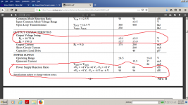
Mark, I am not familiar with the others. If you have access to the AES library it's worthwhile to get this paper, but I shouldn't post it here, its (c)-ted.
Attached is Samuels' own measurement. Boring ;-)
Jan
I have a question about the spectrum graph shown in Groner's paper. The high loop gain lowers the harmonics to somewhere below -180dB, okay. But, can someone explain why is the noise floor is lowered to -180dB? Normally, loop gain doesn't reduce noise, so why does it appear to be doing that in this case?
But, can someone explain why is the noise floor is lowered to -180dB? Normally, loop gain doesn't reduce noise, so why does it appear to be doing that in this case?
Not necessarily the case, huge FFT's and ordinary averaging can achieve that. A reduction of equivalent noise BW of 10 on each bin is a 10dB improvement in the floor. Synchronous averaging lowers the noise floor as the square root of the averages as long as the amplifiers noise is uncorrelated and gaussian (mean = 0).
Like I implied in an earlier post, I've become a bit fascinated with the idea of using conditionally stable composite op-amps to make a low-distortion two-integrator oscillator. As an intermediate step, I've been playing a bit with a root locus program and a pole-zero extraction program trying to find a way to make a composite op-amp from two identical op-amps, for example a dual op-amp (which has the disadvantage of supply, substrate and thermal coupling between the op-amps, but the advantage that it's cheaper and more compact than two separate op-amps).
Today I built up the result on a piece of perfboard, see the attachment. I actually want to use LM4562 op-amps with R3 = 18 kohm and R4 = 1 kohm, but not having any LM4562s in the attic, I scaled everything for an OPA2134 for this first test. Basically R3 and R4 have to be inversely proportional to the gain-bandwidth product of the op-amp, assuming unity-gain-stable op-amps with normal first-order roll-off up to unity open loop gain.
The part between dashes is the composite op-amp, the rest is the feedback around it. I've made a simple inverting amplifier to see if it works at all. Simple functional checks look OK: all bias voltages make sense, there is no hand effect and when I played a Tracy Chapman CD and some dancehall reggae through this amplifier, the tweeters didn't go up in smoke and the music sounded normal. Temporarily reducing R1 to overload the amplifier also didn't cause any disasters.
Attachments
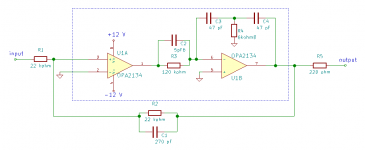
Why R5 so big / what's the smallest R5 that can be tolerated ?
I'm intrigued by 6kohm8 and 5pF6... Not sure that's very common, I assumed the unit only steps inside the number for the unit case (6R8 for instance), not that I've seen 6F8 or 6H8 that I can remember.
Is there even a standard for this engineering notation?
I'm intrigued by 6kohm8 and 5pF6... Not sure that's very common, I assumed the unit only steps inside the number for the unit case (6R8 for instance), not that I've seen 6F8 or 6H8 that I can remember.
Is there even a standard for this engineering notation?
Hmmm, it appears moderators merged questions from post #236.5 (now deleted) and #236. I wrote the first paragraph of #236 , I have no idea who wrote the 2nd and third paragraphs except, I am sure it wasn't me. Leftover cruft from a deletion and attempted merge, methinks.
Hmmm, it appears moderators merged questions from post #236.5 (now deleted) and #236. I wrote the first paragraph of #236 , I have no idea who wrote the 2nd and third paragraphs except, I am sure it wasn't me.
According to a notification I received it was @Mark Tillotson
I haven't a clue how low R5 could be, probably about the same as for a conventional OPA2134 voltage follower. It could obviously be 0 ohm without any capacitive load, but as I'm driving a 5 m-long cheap cable, I just picked a value that's likely to be much greater than the open-loop output impedance of the OPA2134.

- Home
- Source & Line
- Analog Line Level
- Samuel Groner's super opamp