The 9610/610 have 25C 1.8A and 100C 1A drain current DC absolute max spec. Means their core will handle 1.8A to 1A between 25-100 degrees Celsius. Core is hotter than the outer case and sink. At 258mA you have plenty of headroom before challenging those specs. In general, for reliable long term operation and acceptable home hi-fi temperature, look for no more than 55C on the UBiB sinks.
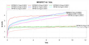
They also state different enough Ciss Coss Crss in their datasheets. So they are same power class mainly but not the same die. Especially in such low test Id for Mosfets there will be more pronounced differences in curves between not exactly same parameter types.

I have done some more measurement according to your suggestions and I found VGS for M1=FQP3P20 is 5,15volts, Vbe for Q1=BC-327-40 is 0,The Leds shouldn't change brightness as you adjust the Vout pot. They are supposed to use constant current. Check Q2 Q3 for a start.
62volts. Voltage over R4 is 0,57volts. With that I think this first section working pretty correct.
Next section is voltage over R5 0,17 and voltage over R6 is 0,17 Vbe for Q2 BC560 is ca 1volt and Q3 is 4,5volts and voltage drop over R7 is zero. And the leds light up.
Last section (may suffer from previous stage) M2=IRF530 VGS= 0,42volts no voltage drop over R8 and finally Q4 = BC327-40 Vbe is 1,03volts.
All set up for 5volts 100mA and output is ca 4,7volts right now with a 33ohm 3W wirewound resistor as load. I have measured IDSS > 7,5mA at J3 PF5102
Any help or suggestions is most valueable,
Vbe Q1 must be about 0.6V as much as VR1. VR4 suggests normal 2mA Q1 bias. VGS FQP is normal for the type at over 5V. So yes, your CCS section looks like working correctly.
Vbe Q2=VR5. Normally about 0.6V. Something's wrong with Q2 and/or Q3. VR7=0 shows no bias current. Pull out & measure/replace Q2 Q3.
If they will prove good, then J2 must be bad not biasing them.
Last section may suffer from the previous stage indeed. When it will fully work expect 3.5-4V VGS from the M2 IRF at this range of settings.
Thanks Salas. I will pull out those. Anny method for measure them (Q2 & Q3) without an transistor tester?
I have pulled them out and done some diode testing and seems to work ok PNP testing with negative on base and ca 0,7volttage drop on both emitter and collector nothing the other way. Will now look at J2Thanks Salas. I will pull out those. Anny method for measure them (Q2 & Q3) without an transistor tester?
That test is sufficient to just know if transistors are broken or not. Nothing about meeting spec. Maybe its enough of a test for now.
J2 because a JFET it takes an Ohm meter to compare its RDS with healthy ones of same type and alike IDSS. RDS magnitude is inverse to IDSS. Must not read near a short neither in the kΩ.
If you will not find bad semiconductors in any section, there could exist a layout bug if its your own design board on first time assembly. Verify all connections proper vs the schematic with the DMM's continuity beeper.
Salas the output is 4.9V and Cronus needs 5V, also the power R-Core 9V 30VA makes mechanic noise?
4.9V should be within any 5V nominal gear's tolerance of operation. Why's 4.9 fixed? Using only Leds? No output voltage trimmer installed?
Chinese R-Core or older French shop sourced one? What are those graphs showing, what is red and what is yellow?
Chinese R-Core or older French shop sourced one? What are those graphs showing, what is red and what is yellow?
It's a mobile app to measure sound pressure & frequencyWhat is measured? Audio output? Power rail? Is that a mobile phone screen capture?
The R-Core never did any mechanical noise, it's Silchar from India bought to french web shop.
YesYou use a microphone to measure TX mechanical noise? That's what we see in the graphs?
- Home
- Amplifiers
- Power Supplies
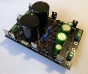
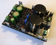
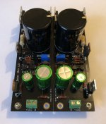
- Salas SSLV1.3 UltraBiB shunt regulator