1MHz is way far from the 13.23MHz gremlin you scoped
I agree. I was just curious about your compensation strategy because you're cutting it so close lower down. Of course, SPICE is not necessarily reality.
-Henry
I didn't read your earlier message carefully enough, the one where you mentioned gate resistance. I have a feeling if I put some 100 Ohm SMD gate resistors right on the LSK170 gate pins it would solve the problem...
LOL, nice. I see what you mean.
It's working nicely now, both with phones and in the living room system. I'm listening to it now with the cans, actually. Sounds good. I think I'll do some SPICE on my own, see what insights I can came up with. Mysteries are opportunities for learning.
-Henry
It's working nicely now, both with phones and in the living room system. I'm listening to it now with the cans, actually. Sounds good. I think I'll do some SPICE on my own, see what insights I can came up with. Mysteries are opportunities for learning.
-Henry
Notice the op-amps rivaling high but wide OLG also from just a simple two stage system.
P.S. LSK models in the Spice sim were Cordell published
P.S. LSK models in the Spice sim were Cordell published
A small capacitor from the output to the far side of R4 kills the oscillation.
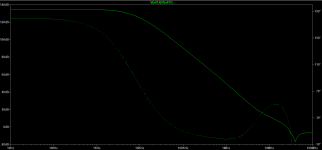
If your SPICE plot is to be trusted, you have two poles at around 10kHz and almost no phase margin. I don't think the high-frequency end of your plot is necessarily representative of the circuit in the real world.
Increasing the value of C2 doesn't help, as expected.
A lag network around M1-M2 should split the poles, but I've done neither measurement nor simulation to get an estimate of the effect. It doesn't sound any different to my ears with or without the compensation caps. But no oscillation, of course. I will try to get a SPICE model going tonight.
Maybe a more aggressive Zobel on the output would have the same effect, dunno.
With this high GBW, it makes sense compensation might be fiddly.
-Henry
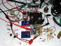
It's not a new development for me. Tested very well on its breadboard then on its standard board. Has been also built so many times by other people in that form without problems too that I am not inclined to change something because of Spice suggestions. It doesn't know what the board does to the circuit. You do well looking further into your implementation of course.
Having the experience of the development I suggest first thing is to try gate stoppers in your input JFETs. Spice would show a more degrees earlier than -1 (0dB) curve with 330pF C2 for instance but in practice I was only making it oscillate beyond 68pF. So it should be more reliably indicating around zero gain because it steals margin there in the sim too with more C2 pF.
I could try a Nyquist plot analysis too since -180 deg at G -1 is the instability point not just low phase points suggested along the phase line but I prefer the real thing experience since it was there before. Scoped, pulsed, loaded with cans and line gear etc.
I could try a Nyquist plot analysis too since -180 deg at G -1 is the instability point not just low phase points suggested along the phase line but I prefer the real thing experience since it was there before. Scoped, pulsed, loaded with cans and line gear etc.
Actual gain-phase plots from measuring the circuit in real life would be very instructive. I don't have the instrumentation to do that though.
But the most weird point still is why a gremlin on one channel and not on the other. Any theoretical or practical Bode or Nyquist OLG plot should equally apply to both channels.
It's possible the circuit is conditionally stable and I got unlucky. When I get my SPICE model going I will have a better idea.
Did you also check if the PSU rails are clean and stable? In case its an interaction. +Rail line goes straight down to the M2 cascode MOSFET's gate with a divider for instance.
Probing the rails with AC coupled scope on mV vertical scale and moving across the horizontal from slow to very fast sweep should catch riding waveforms if any.
Probing the rails with AC coupled scope on mV vertical scale and moving across the horizontal from slow to very fast sweep should catch riding waveforms if any.
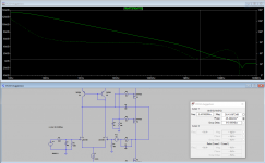
You probably will hate this, but I quickly threw together a SPICE model. The results match pretty well with what you posted earlier, including the alarming midband phase dip.
I then added my 22pF compensation capacitor. This happened to be the one reasonable value I had in my junk box. You can see it drastically splits the poles, increasing the minimum phase margin to 45 degrees. It's actually over 60 degrees at the unity gain crossover point, though the drop above 20MHz might be an issue.
As before, I'm not at all confident of the accuracy of these simulations at higher RF frequencies. But this is something to think about.
The downside, of course, is a significant loss of open-loop gain over much of the audio band due to the much lower corner frequency. Whether or not this is audible is another question.
-Henry
Attachments
It will promote more treble distortion when losing open loop gain in the audio band. If audible it may sound harsher or brighter but compensate as you wish. Me I would have first tried gate stoppers on J1 J2.
Your design credentials are stellar, Salas, especially compared to mine, so please don't take this the wrong way. ASSUMING the SPICE simulation is at all accurate, even in my aggressively-slugged circuit there's still 75dB of loop gain at 20kHz. This is an absurd amount of gain and though it's possible, there's no guarantee the increase in distortion would be audible. On the other hand, again ASSUMING the SPICE is correct, the uncompensated circuit has a serious phase margin issue at low RF frequencies. And this could, in fact, introduce some hard-to-measure and hitherto unsuspected transient distortions that themselves would be audible.
I heard no difference whatsoever when switching in the 22pF caps while listening. Which means nothing because neither my headphones nor my ears are reference-caliber.
I think this bears further investigation. Of course lots of people have had good results with your circuit, and you can't argue with success.
This would not even be a question if my prototype weren't oscillating.
-Henry
The 13.23MHz waveform found in one of your build's channels still does not compute with much lower frequency poles. Or why nothing on the other channel or why nothing when with headphones as a parallel load. Headphones lower the load impedance a lot vs line level. Can they be also lowering RF susceptibility in the FB node to J2 (?).
I wouldn't slow down the circuit before checking PSU rails are pure and parasitic inductance damping is good on the input pair's gates. But that's just how I usually debug. Starting with the odd scenarios. But its your build on your layout you decide how to settle it.
As you saw I had also Spice analyzed in the past about this originally bench developed and bench tried circuit. With very alike plots. But I did not tweak it on Spice reference since even there it never goes to G=1 with 180 degrees phase shift. That's the instability criterion. Other things may be called sensitivity in control theory and I don't trust those generic MOSFET models are spot on especially when there is no layout parasitics info in my simulation to even start thinking of meaningful Nyquist plotting.
Since it sounds as I like it and it was stable live with the compensation I chose on the bench with the input filter I chose on very fast square waves, nF capacitor output loading, various headphones, tried in beta testers racks as line preamp on various power amps etc.
Is it like a modern fighter jet needing to be on stability's edge to can turn on a dime? Maybe. Must be made on official PCBs and better with PSUs I designed and tested it with to surely perform as expected? Maybe. But it also worked on several occasions with differentiated artwork before. Anyway, if quirky at all I at least liked how it fights. 🙂
I have no complaints, Salas. I guess this is my own project heavily inspired by the DCG3, hah.
I just soldered the 22pF compensation caps to the back of the board because I wanted to make sure it was the caps (or cap, since it's only one side) making the difference and not the two feet of wire clip leads. The board is stable, but I find if I put my finger on the gate end of R1 it breaks out again -- though it's oddly inconsistent. There's no sign of instability on the other channel.
One difference is I'm running 150 Ohms for R3 on both sides and the J3 on the "bad" side is weaker... So I have about 4.4mA total bias current on that side, and 6.6mA on the "good" side -- though I don't see how that would matter.
The board layout is as close to symmetrical as I could make it. I do think gate stoppers are a good idea. I need to see what SMD resistors I have lying around and do some more surgery.
-Henry
- Home
- Source & Line
- Analog Line Level
- Salas DCG3 preamp (line & headphone)