buddy,Hi all,
I'm new to this thread...!
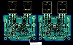
This is my 1st amplifier layout. I've been working with small layouts earlier.But this one seems to be a BOMB!
Any Suggestions related to placement of components welcome!
Thanks and Regards
Mark
P3A original PCB layout is no more a secret. Its there in the internet. somebody have already posted it. if you have basic skill in Photoshop, you can easily replicate the original layout. I have already done that. (but I am not going to post it anywhere because I dont like to help anybody loot such a great man Rod Elliot.) if you are doing it for the sake of doing it, that is a different story.
This guy is mad.what's wrong with some truth? The truth will proverbially set you free.
Rod is neither compelling anybody to construct his designs . He designed something, he believes it works. thousands build his designs and nobody make a complaint. why throw mud upon a man like Rod as long as he is offering his designs for free? forget his amps. they may be substandard (or not!) what about the information he provide in his website? I havent yet paid him a penny for all that I have downloaded from there. (thank you Rod.) If you think his designs are substandard as you think, make something superior to them and distribute it free to the world like Rod do.
until then leave him alone.
so many words....what does it amount to?🙁🙄
why can't AndrewT just show us in pictures what he's got so we can appreciate what he says....
In answer to your questions, I have a Novel idea, why don't you Ask Andrew ?
Maybe he can get you a few snappy shots ?
As to appreciation, it is a personal taste.
There was a site dedicated to P3A, Andian Audio. The guy that built P3A using original ESP pcbs measured:
S/N >100dB 20-20,000Hz
Distortion <0,009%
PSRR 48dB
Hum -94dBV at idle
DC offset 30mV max
Considering the simplicity of the circuit these are excellent results.
S/N >100dB 20-20,000Hz
Distortion <0,009%
PSRR 48dB
Hum -94dBV at idle
DC offset 30mV max
Considering the simplicity of the circuit these are excellent results.
I think it wasAndian Audio have a website? I did a search on Google and nothing appears.
Regards
http://www.anidian.com/audio/construct/p3a_1.shtml
offline when I checked today, but you can find references to it in this forum.
Thanks. Are Anidian, no Andian, for this I can not find. But the link say: ERROR 404 - PAGE NOT FOUND.
Regards
Edit, this are the correct link:
http://web.archive.org/web/20030801075806/http://www.anidian.com/audio/construct/p3a_1.shtml
Regards
Edit, this are the correct link:
http://web.archive.org/web/20030801075806/http://www.anidian.com/audio/construct/p3a_1.shtml
Last edited:
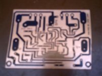
.....The attachment shows more suggestions.....🙂
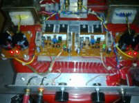
Good day sir Alex sir... sir pls. check my p3a amp if im mistake sir because not work i use +/- 24V DC rails..
Attachments
I doubt you'd ever measure P3a distortion as low as quoted by Andian Audio. That seems more in the order of simulated results or using fabulous quality parts rather than the old industrial power transistors they specified. 'Best I have seen with a sound card, is 0.05%/ 50W 8R with MJL3281/1302, an average build with conventional diodes and wiring standard.
I'm sure you can tweak distortion down if you want to but not many have the gear to do this, so it's down to following general advice and hoping that's good enough, for most builders. Using the P3a's constant-beta output transistors, Rod still only specifies 0.04% THD. That's actually still very good for the design's weaknesses and simplicity.
The point about taking Rod's designs and posting them eveywhere over the internet has been raised and answered many times: The designs and specifically the PCBs he makes are his livelihood, income, business etc. He's a member here like us and asked a few times that we respect his IP by linking to his website rather than copying his webpages and other schematics and data to the forum. There has been a longstanding agreement I understand for the forum to abide by that
You disagree? - think all information should be free like in Utopia or some country where there is no worthwhile technical information? - too trivial a design or unimportant to restrict?.
Stiff luck, Dudes. The forum rules don't accept copyrighted material posts. You see them here with logos still on them and sure, moderators don't see all posts or check everything. I think if there are rules, then read and observe them, whatever you think. We are visitors here - we own no rights to the IP of others unless they specifically grant permission. What you do with the materials available on other websites is entirely your responsibility. However, if the forum rules says not here please, then break the rules somewhere else rather than trash other people's efforts to keep them.
D
Deleted member 148505
Good day sir Alex sir... sir pls. check my p3a amp if im mistake sir because not work i use +/- 24V DC rails..
Check the pin orientation of the transistors you used...
Good day sir Alex sir... sir pls. check my p3a amp if im mistake sir because not work i use +/- 24V DC rails..
"Not working" is a bit unhelpful. What are the symptoms ? Do you blow fuses ? Is there DC on the output ?
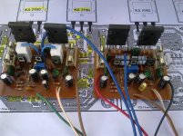
In the first picture, the amplifier on the left has a fake MJL21193. What other transistors have you used? Are you sure they are genuine parts?
Good day sir Alex sir... sir pls. check my p3a amp if im mistake sir because not work i use +/- 24V DC rails..
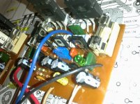
Hi desertstorm .
In this morning i had test this board.
Take a look on green led.
Anode(long pin) must be connected to base of bc546.
Pcb is wrong at this point at least.
I don't know for other mistakes .
Regards.
Attachments

Last edited:
Check the pin orientation of the transistors you used...
thanks sir Problem solve sir its a fake bd 140 and led pins orientation now woking fine sir i make also my own PCB sir based on sir eliiot p3a and circuit diagram by sir Davide Bucci works fine sir...
Last edited:
Hi desertstorm .
In this morning i had test this board.
Take a look on green led.
Anode(long pin) must be connected to base of bc546.
Pcb is wrong at this point at least.
I don't know for other mistakes .
Regards.
Sir heres my own pcb based on sir elliot P3A and circuit diagram by sir Davide Bucci working fine sir..
Attachments

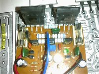
No heatsink for the driver transistors or thermal coupling for the bias transistor? That will be "interesting" under power, or is that just a part finished amplifier?
Hint: bias will be irregular and too slow in response, without enough thermal coupling to the driver(s).
Being right next to the output emitter resistors, they will have more affect on bias than the drivers. This is not a good layout for a CFP amplifier design. It may be possible to move the large resistors under the board and simply kink an aluminium strip heatsink to fit to the correct side of the righthand driver transistor (as in pic 3, above). This should solve the problem of what looks like reverse facing drivers.
Thermal coupling can be done by having a small bias transistor in close proximity, as you see on Rod Elliott's original PCB or a larger one fixed to the same heatsink as in AlexMMs layout. If you use TO126 transistors for all 3, as you have, it would be much better to couple them all to the same small heatsink, which could be a simple strip of 3mm aluminium, perhaps 15 mm wide.
Last edited:
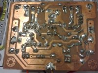
My layout is bad, check the elco!
Hi Ian,
thanks for the tip...
too bad my layout is not so good.
I've make a new one & again I guess it is not so good but I will try it.
It is stereo board, but I will not post here
I check again my previous layout (post #228) & there so many error there so please don't use it,
It is a miracle if it is can be used 😀. Sorry if anyone try it & fails
Regards
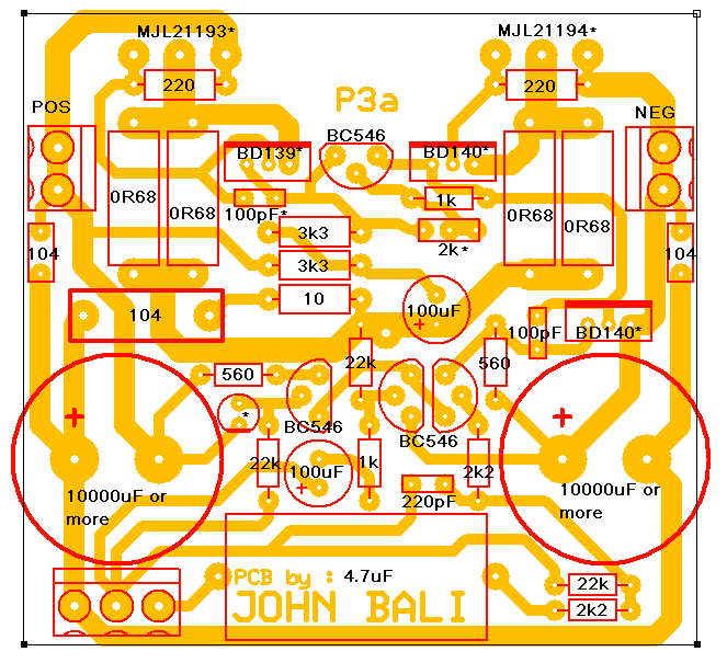
John,
the big space where P3a is printed is where the power +ve, power -ve and power ground should be located. The HF decoupling should also be located here giving the shortest route from output emitter to output emitter.
the big space where P3a is printed is where the power +ve, power -ve and power ground should be located. The HF decoupling should also be located here giving the shortest route from output emitter to output emitter.
Hi Andrew,
My new layout is so different with this one & thanks for your suggestion, you really help me.
Now that newest one has already made the pcb by myself (home made pcb)
I hope you & Sakis will be like that one
but I don't post for any P3A layout anymore.
I will post the result here : http://www.diyaudio.com/forums/solid-state/164756-p3a-comparsion-table-long.html
because I want to compare some transistor too 🙂
Regards
No heatsink for the driver transistors or thermal coupling for the bias transistor? That will be "interesting" under power, or is that just a part finished amplifier?
Hint: bias will be irregular and too slow in response, without enough thermal coupling to the driver(s).
Being right next to the output emitter resistors, they will have more affect on bias than the drivers. This is not a good layout for a CFP amplifier design. It may be possible to move the large resistors under the board and simply kink an aluminium strip heatsink to fit to the correct side of the righthand driver transistor (as in pic 3, above). This should solve the problem of what looks like reverse facing drivers.
Thermal coupling can be done by having a small bias transistor in close proximity, as you see on Rod Elliott's original PCB or a larger one fixed to the same heatsink as in AlexMMs layout. If you use TO126 transistors for all 3, as you have, it would be much better to couple them all to the same small heatsink, which could be a simple strip of 3mm aluminium, perhaps 15 mm wide.
thank you so much sir Ian for your comment and advise..more power to you sir.
- Home
- Amplifiers
- Solid State
- Rod Elliot P3A Layout - Critics