D
Deleted member 148505
Put it this way, Tekko - Rod sees a lot of copies of his boards because people think an auto- router in their PC software can do just as good and looks pretty, nice and close together etc. I've made PCBs by hand, artwork and cheap or free software for a lot of years but I can assure you that in hi-end audio and RF work, nothing is as good as someone who knows best spacings and position of parts, track alignments, thermal gradients, EMR patterns and who is designing for A1 performance with the skill and experience for it.
Typically, you can halve THD by smart trackwork in the output transistor traces and feedback routing. You can reduce noise by parts selection and location. Yes, you can learn that there are do's and dont's rules to follow like star grounding paths but do we know how much is necessary for optimum performance of the design? After 10-20 iterations and feedback, you might be getting somewhere. Rod has that experience with his very old designs but I don't think many people see it. It can make that difference between 500 Euro and 5,000 Euro amplifiers and of course, the odds you will ever get paid for any design. There are guys here who are breathtakingly good at commercial work but you see something else when you look inside the best fancy brands.
For "mission critical devices", I agree that optimal layout for pcb is required.
But for class AB amps, I think the performace gain of very good layout is negligible for normal listening, for me, as long as "other layout's" performance is within -5% or -10% of the measured specs of commercial pcb layout, then it is forgivable...
D
Deleted member 148505
given the chance to talk about it ..... if you willing to design a pcb for a simple device like the P3a and follow all the mentioned rules above, and some others not mentioned in this thread is actually impossible ( trust me on this one been trying for 5 years in my spare time )
you may as well go for a double layer but then you are swimming in unknown waters like proximity where induction or capacitance between traces and layers will be impossible to evaluate properly for people that don't have experience and/or highly sophisticated equipment .
Conclusion is that you have to "keep" the rules but up to a certain point divided by symmetry /looks and all of it underlined with the cost factor ...
conclusion also is that people that exist in the diy often are bad in mathematics ( like me ) so the above equation is almost impossible to solve ....
happy regards
sakis
Yes, as they said "we do not live in an ideal world", we can't have it all, so even in pcb design, we have to make compromises in the design...
I agree with both of you really. The point about P3a in particular, is that it is an old, nasty CFP design from the early days of silicon. These always sound bad when biased at "optimum'" 12mA and it just so happens that with a bit of tweaking, more bias, and care with bias control, this piece of junk sounds like a million dollars. There are commercial amps (e.g. Hitachi) with this high bias scheme too and their owners here still love them so I get to fix a few and play with SQ/bias (fun!).
I am almost retired but I teach some noob kids how these layouts and builds can be done and I know at that level of comparison to Rod's latest board, the differences (apart from parts errors and disasters) is often quite a lot in the SQ. Sure, a lot of guys are just happy to have a cheap, working amp with plenty of power. We can get this anywhere and cheap, too. I like a few designs specially because, despite all the engineering "faults", these do what we would like them to do - just that bit sweeter and more interesting, so we feel great when we listen and all that hi-end talk. I don't judge anybody's work here and I hope your design sounds great when you finish tweaking, jlester.
I am almost retired but I teach some noob kids how these layouts and builds can be done and I know at that level of comparison to Rod's latest board, the differences (apart from parts errors and disasters) is often quite a lot in the SQ. Sure, a lot of guys are just happy to have a cheap, working amp with plenty of power. We can get this anywhere and cheap, too. I like a few designs specially because, despite all the engineering "faults", these do what we would like them to do - just that bit sweeter and more interesting, so we feel great when we listen and all that hi-end talk. I don't judge anybody's work here and I hope your design sounds great when you finish tweaking, jlester.
D
Deleted member 148505
Hi,
Here's the revised layout...
Suggestions are welcome...
Here's the revised layout...
An externally hosted image should be here but it was not working when we last tested it.
Suggestions are welcome...
D
Deleted member 148505
I don't judge anybody's work here and I hope your design sounds great when you finish tweaking, jlester.
Hi, I already listened to my P3A (the one I posted earlier), and now it's my best sounding amp at home even without tweaks. Thanks 🙂
It beat my current and previous amps using the same speaker: av-735, tda8950, jvc ax-r97, onkyo tx-nr900, LM3875 and LJM L25D
I will try leach amp and techno amp next 🙂
Last edited by a moderator:
D
Deleted member 148505
Here it is 🙂, I replaced the stock amp of JVC AX-R97 with the p3a. Definitely sounds better than the original.
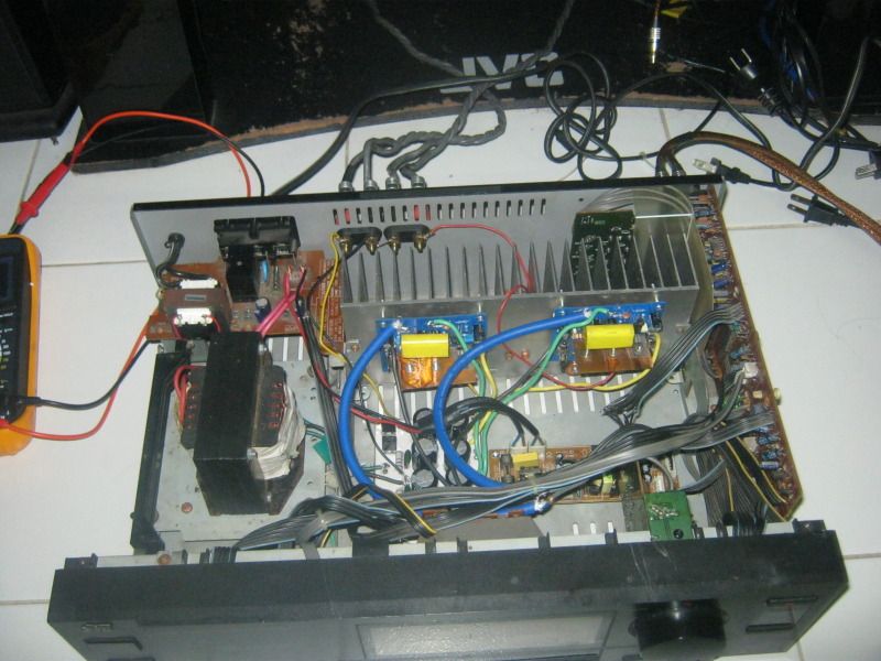
PS: the speaker wires are just temporary 🙂 I'll diy another one...
PS: the speaker wires are just temporary 🙂 I'll diy another one...
D
Deleted member 148505
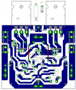
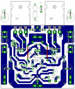
Here's my new layout for p3a
Added base stoppers for drivers and output transistors and added VBE CE bypass cap
Added base stoppers for drivers and output transistors and added VBE CE bypass cap
Attachments

Last edited by a moderator:
Your sch is pretty good.
I would add more emitter resistors, LTP, VAS
Limiting resistor in series with VR1.
D.Self resistor between R16 and Q9 collector. As used by quite a few other designers.
R//L on output.
I like your input and your Signal Ground.
C6 might be better with a series R and then maybe duplicated for Q5. Easier to omit than to add.
Layout.
I hate your separated +ve & -ve supplies.
The decoupling is far too far away from the main current consumers. They should be in a tight loop around the Q7&8 emitters.
Last edited:
Well. needing stopper resistors, if that is really the case, does not indicate it's close enough at all. Instability is caused by the inductance of long traces, where they should not be. P3a does not need stoppers, so it would be better, whilst you are redrawing, to shorten traces there as much as practical and decouple as AndrewT suggests..... close enough same amp different name
Here's my new layout for p3a
Added base stoppers for drivers and output transistors and added VBE CE bypass cap
hello, your design seems very good, now my question is: if you replaced the transistor that adjusts the quiescent current, I have assembled this circuit and the PCB put a transistor "BC546" as in the original scheme. had some problem with the quiescent current and its fit with the transistor "BD139"? thanks and regards.
D
Deleted member 148505
Your sch is pretty good.
I would add more emitter resistors, LTP, VAS
Limiting resistor in series with VR1.
D.Self resistor between R16 and Q9 collector. As used by quite a few other designers.
R//L on output.
I like your input and your Signal Ground.
C6 might be better with a series R and then maybe duplicated for Q5. Easier to omit than to add.
Layout.
I hate your separated +ve & -ve supplies.
The decoupling is far too far away from the main current consumers. They should be in a tight loop around the Q7&8 emitters.
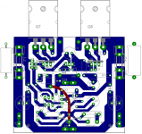
I think I need to expand the pcb size to accommodate your suggestions. Can you please help/teach me calculate the required values if ever? 🙂 For decoupling I saw some pcb designs like baksa and techno and they are all far away from output trannies so I thought it's ok to leave it there..
BTW here's the updated layout and schema... =)
An externally hosted image should be here but it was not working when we last tested it.
An externally hosted image should be here but it was not working when we last tested it.
Last edited by a moderator:
D
Deleted member 148505
hello, your design seems very good, now my question is: if you replaced the transistor that adjusts the quiescent current, I have assembled this circuit and the PCB put a transistor "BC546" as in the original scheme. had some problem with the quiescent current and its fit with the transistor "BD139"? thanks and regards.
I already tried bd139 as VBE multiplier for P3A (see my previous posts) and I didn't encounter any problem... It is also easier to mount on a heatsink altogether with the drivers.
Yes, using those examples would be a good idea except that generally, EF2 designs don't have many instability (oscillation) problems. However, CFP can be a problem with any added inductance and so it is wise to take extra precautions with the layout. The same goes for triples and any high gain output stage........ For decoupling I saw some pcb designs like baksa and techno and they are all far away from output trannies so I thought it's ok to leave it there..
My suggestion is not to increase the size, but move the drivers much closer to the output transistor connections. Bolt the Vbe multiplier direct (but insulated) to either driver heatsink for simplicity. Of course, a single heatsink for all 3 semis would be ideal. Keep going, I think you are proceeding very well.
So, did you actually find any oscillation on the scope or otherwise?
D
Deleted member 148505
How about placing a wirelink under the pcb so that decoupling can be placed near output trannies? I removed the base stoppers because I assumed it will be stable.
Attachments
Last edited by a moderator:
The HF decoupling has to go there as well, and they have priority for absolute shortest route length.
Then connect the decoupling ground to the power ground.
Then connect the decoupling ground to the power ground.
D
Deleted member 148505
Or I will just make decoupling (near output tranny) optional? Will put them if the amp is not stable.
Is there a scenario where the amp is stable in normal condition and unstable in transient ones?
Is redundant decoupling/bypass ok?
Thanks
Is there a scenario where the amp is stable in normal condition and unstable in transient ones?
Is redundant decoupling/bypass ok?
Thanks
Attachments
Last edited by a moderator:
Yes, fast signals can make the output unstable, or at least not follow the signal as well as normal.
This can be eased by designing the amplifier to cope with fairly fast signals. And then follow that up with an effective RF filter at the input.
This can be eased by designing the amplifier to cope with fairly fast signals. And then follow that up with an effective RF filter at the input.
I may have missed on space for a component or 2 but it seems obvious to me from the the last few PCB patterns, that Q5,6 could both be moved up towards the output transistors - about level with the collector of Q4. That would give more compact and tidier output stage tracks and the collector ballast resistors could also now go closer to make room for this.
- Home
- Amplifiers
- Solid State
- Rod Elliot P3A Layout - Critics